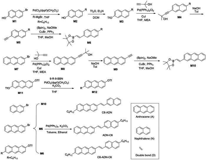
Scheme 1.
Synthetic route to anthracene derivative of C6-AND, AND-C6, C6-AND-C6.

Thermally stable organic ultrathin single-crystal field-effect transistors based on anthracene derivatives
Yingying Hu , Yanan Sun , Dawei Liu , Zhilei Zhang , Chunlei Li , Jie Liu , Lang Jiang


Organic semiconductors (OSCs) are promising candidates for the next generation optoelectronic devices and have found widespread applications in organic field-effect transistors (OFETs) [1–4], organic light-emitting diodes (OLEDs) [5–7], organic photovoltaics (OPVs) [8,9], and photodetectors [10,11], etc. Owing to their excellent signal amplification capability, flexibility, lightweight nature, and low cost, OFETs have great potential for applications in drive circuits, wearable electronics, and sensors [12–17]. Nonetheless, the commercialization of OFETs has long been restricted by challenges related to operational stability. In recent years, great efforts have been devoted to enhancing the stability of OFETs, including air stability [18], operational stability [19], and stability under specific conditions, such as high temperatures [20].
Due to the weak molecular interactions in OSCs, their aggregation structures are highly susceptible to degradation at elevated temperatures [21]. Developing OSCs with intrinsic thermal robustness offers a direct pathway to fabricating thermally stable OFETs. Significant advances have been made in recent years toward improving the thermal stability of OFETs [22–31]. Generally, the enlargement of molecular structures could improve their thermal stabilities in OFETs. For instance, decyl-phenyl-substituted DNT-Vs, namely C10Ph-DNT-VW, exhibit high thermal durability up to 180 ℃ [24]. DNTT derivatives were found with superior thermal stabilities, such as OFETs based on 2, 9-DPh-DNTT retain superior OFET characteristics up to 250 ℃ [32]. Another DNTT derivative, DBTTT, demonstrates thermal stabilities in thin-film transistors (TFTs) at temperatures up to 140 ℃ [33]. Among anthracene derivatives, DcHPA with cyclohexyl outperform counterparts with n-hexyl groups, and DcHPA-based devices can preserve 50% of their electrical performance after heating to 150 ℃ [23]. Despite these progresses, most OFET thermal stability has focused primarily on thin-film and bulk crystal devices. In contrast, studies concerning ultrathin single-crystal OFETs remain notably scarce [34,35], highlighting a significant gap and opportunity for future exploration.
In this work, we designed and synthesized three p-type asymmetric anthracene derivatives, C6-ADN, ADN-C6, and C6-ADN-C6, by systematically modulating the alkyl substitution sites to regulate the growth behavior and investigate their thermal stability in OFETs. Crystals with mono-molecular thickness were obtained for C6-ADN-C6, while C6-ADN and ADN-C6 self-assembled into bi-molecular thickness crystals. SCFETs based on C6-ADN, ADN-C6, and C6-ADN-C6 demonstrate the highest mobility of 1.91, 4.05 and 1.30 cm2 V-1 s-1, respectively. The thermal stability assessment indicates that at 140 ℃, the average mobility retention values for C6-ADN, ADN-C6, and C6-ADN-C6 were 48.7%, 81.2%, and 0.87%, respectively. Strategic modulation of the alkyl chain position in asymmetric anthracene derivatives provides an effective pathway for enhancing thermal stability, paving the way for developing high-performance, thermally robust ultrathin SCFETs.
The synthetic routes of C6-ADN, ADN-C6, and C6-ADN-C6 are shown in Scheme 1. The detailed synthesis and characterization as shown in Supporting information.
As the UV-vis spectra shown in Fig. 1a, all compounds exhibited similar UV absorption profiles because of the same π skeleton. The optical bandgaps, derived from the onset absorption wavelengths, were calculated to be 2.90, 2.90, and 2.88 eV, respectively (Table S1 in Supporting information). Cyclic voltammetry (CV) measurements indicated that these materials possess similar electrochemical properties, as evidenced by their irreversible redox peaks (Fig. 1b). The HOMO energy levels were calculated to be −5.57, −5.58, −5.59 eV for C6-ADN, ADN-C6, C6-ADN-C6, respectively (Fig. 1c). Notably, the position of the alkyl substituents has minimal influence on the optical and electronic properties. This conclusion is further supported by frontier molecular orbital calculations performed at the B3LYP/6–31G* level (Fig. S1 in Supporting information).
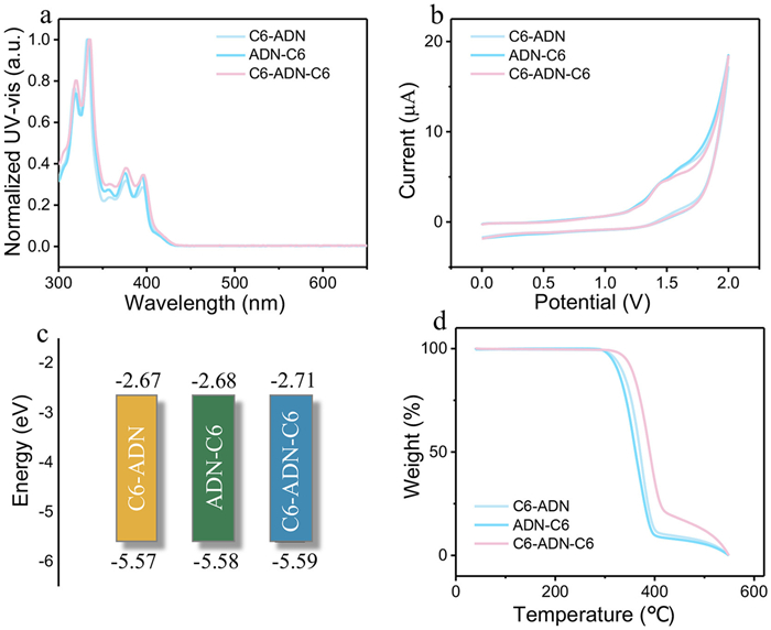
Thermal stability was evaluated using thermogravimetric analysis (TGA) and differential scanning calorimetry (DSC) (Fig. S2 in Supporting information). As shown in Fig. 1d, the decomposition temperatures (corresponding to 5% weight loss under nitrogen atmosphere) for C6-ADN, ADN-C6, and C6-ADN-C6 were 320, 314, and 342 ℃, respectively. A slight increase in thermal stability was observed for the C6-ADN-C6, which correlates with the higher molecular weights.
To investigate their charge transport properties, high-quality ultrathin single crystals were successfully fabricated on SiO2/Sin++ substrates via a drop-casting method. As shown in Figs. 2a, e, and i, the crystal morphology of the three materials is irregular hexagonal. Under polarized optical microscopy, the crystals display uniform coloration, confirming their single-crystalline nature (Figs. 2b, f, and j). AFM measurements revealed crystal thicknesses of 4.6, 4.5, and 2.6 nm for C6-ADN, ADN-C6, and C6-ADN-C6, respectively (Figs. 2c, g and k). Notably, the thicknesses of C6-ADN and ADN-C6 crystals correspond approximately to bi-molecular lengths, while C6-ADN-C6 is equivalent to the length of mono-molecular thickness. In addition, the layer-by-layer growth behavior with a bilayer step of C6-ADN and ADN-C6 is also confirmed by the multilayer crystals in Fig. S3 (Supporting information). XRD patterns of the crystals, shown in Fig. S4 (Supporting information), exhibit sharp diffraction peaks and a smooth baseline, confirming the high crystallinity of these samples. The smaller full-width at half-maxima (FWHM) values of ADN-C6, as presented in Table S2 (Supporting information), suggest a higher crystalline quality compared to C6-ADN. Besides, the presence of equally spaced diffraction peaks indicates lamellar growth of molecules in crystals. The interlayer d-spacing is 5.1, 5.0, 3.2 nm, calculated using the Bragg equation (
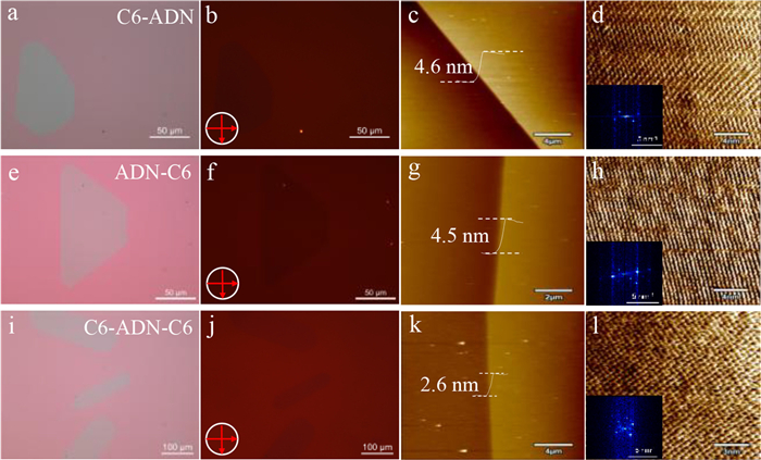
To further resolve the in-plane molecular packing, High-resolution AFM (HR-AFM) and corresponding two-dimensional fast Fourier transform (2D FFT) analyses were conducted (Figs. 2d, h and l). The lattice parameters, derived from 2D FFT patterns, are as follows: a = 0.56 nm, b = 0.78 nm, θ = 90.25ο for C6-ADN, a = 0.59 nm, b = 0.80 nm, θ = 89.65ο for ADN-C6, a = 0.58 nm, b = 0.74 nm, θ = 90.66ο for C6-ADN-C6. The sharp FFT diffraction spots further corroborate the high crystallinity of the three materials. Based on the above information, it can be concluded that while alkyl substitution sites exert a minor influence on packing motifs along the short molecular axis, they play a decisive role in governing growth behavior along the elongated molecular axis. The ultra-thin thickness of the crystals is also beneficial for OFET study.
Crystal structure simulations were performed based on the XRD and HRAFM data. Detailed theoretical calculations are provided in Supporting information. Ultimately, we determined the single-crystal structures of all three systems (Fig. S5 in Supporting information). In addition, the molecular packing diagrams of three systems are presented in Fig. S6 (Supporting information), which can provide direct visual evidence that the position of alkyl substitution influences growth along the long molecular axis.
Based on the crystal structures obtained by simulation, the hole transfer integral (Vh) values between the central were calculated and the details are provided in Supporting information. As shown in Fig. S7 (Supporting information), in the crystal structures of all three systems, the molecules adopt a herringbone packing arrangement. The values of the hole transfer integral are shown in Fig. S7, that is, the hole transport is mainly π-π packing ADN supplemented by herringbone. Moreover, the π-π packing transfer integral value of the former is more than twice that of the latter. In the bilateral alkyl-substituted system (C6-ADN-C6), the hole transport is mainly asymmetric herringbone packing, and the transfer integral values of other transport pathways are relatively low, indicating that there are fewer effective transport channels. This also indicates that ADN-C6 has better charge transport properties than the other two compounds.
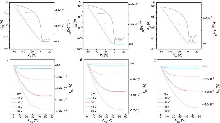
To study the charge transport behavior of ultrathin single crystals. Bottom-gate top-contact (BGTC) SCFETs were fabricated by transferring gold stripes as source and drain electrodes, as shown in Fig. S8 (Supporting information). All devices were characterized at ambient conditions (room temperature, 10%–20% relative humidity). The typical transfer and output curves of C6-ADN, ADN-C6, and C6-ADN-C6 devices were evaluated as shown in Fig. 3 and Fig. S9 (Supporting information). The device exhibits ideal transistor performance, including gate-independent mobilities, nearly zero threshold voltages (Vth), and negligible hysteresis, especially for C6-ADN, ADN-C6 (Fig. S9). The mobility distributions for C6-ADN, ADN-C6, and C6-ADN-C6 based on 30 devices are summarized in Fig. S10 (Supporting information). The average and maximum mobility are 1.44 and 1.91, 2.65 and 4.05, 0.64 and 1.30 cm2 V-1 s-1 for C6-ADN, ADN-C6, C6-ADN-C6, respectively. Among these compounds, ADN-C6 exhibits the highest charge carrier mobility, while C6-ADN-C6 crystals with monolayer thickness show lower mobility. This relatively inferior performance could be attributed to the mono-layer crystals grown on the high surface energy SiO2 substrate may suffer higher interfacial defects and deteriorate the mobility of monolayer crystals [38,39]. The interface trap density is calculated as shown in Table S3 (Supporting information). It can be seen that C6-ADN-C6 exhibits a higher defect density compared to both C6-ADN and ADN-C6. Operational stability was further evaluated through repeated cycling under a continuous square-wave gate voltage at a constant drain-source voltage of −60 V. As shown in Fig. S11 (Supporting information), the output current remains highly stable over multiple cycles for C6-ADN and ADN-C6 devices. In contrast, C6-ADN-C6 exhibits a progressive decrease in current with cycling, underscoring its inferior operational durability.
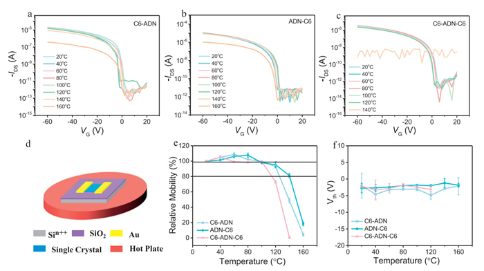
To explore the thermal stability of C6-ADN, ADN-C6, and C6-ADN-C6 SCFETs, in situ testing was conducted. The structural schematic diagram is shown in Fig. 4d. The single-crystal device is placed on a precision digital thermostatic hot plate. The transfer curves and the mobility statistical analysis at different temperatures, as shown in Figs. 4a–c and e. Transfer curves in the temperature range of 20–160 ℃ were recorded for C6-ADN and ADN-C6, while C6-ADN-C6 SCFETs completely degraded at 140 ℃. As shown in Fig. 4e, for C6-ADN and ADN-C6 devices, a mobility increase was observed in the temperature range of 20–60 ℃ and 20–80 ℃, while C6-AND-C6 SCFETs show a slight mobility increase when the temperature is raised from 20 ℃ to 40 ℃. The increase in mobility during the initial heating process might be due to the thermal activation effect. The temperature provides more energy for the molecules in the lattice, making it easier for them to overcome the potential barrier and promoting better charge transport. Obvious mobility degradation happened when testing above 100 ℃. At 140 ℃, the average mobility retention values for C6-ADN, ADN-C6, and C6-ADN-C6 were 48.7%, 81.2%, and 0.87%, respectively. The better thermal stability of ADN-C6 towards C6-ADN might be attributed to its better crystallinity and low defect density (Tables S2 and S3). Nevertheless, to conduct a more effective comparison of the thermal stability of the various isomers, we introduced a quantitative metric, T8n, which is defined as the temperature at which the mobility degrades to 80% of its initial value (Fig. 4e). As summarized in Fig. 4e, T80 values for C6-ADN, ADN-C6, and C6-ADN-C6 were determined to be 127, 142, and 113 ℃, respectively. This indicates that bilayer crystals have better thermal stability than monolayer crystals. To further validate this conclusion, thermal stability tests were conducted on the bi-layer crystal of C6-ADN-C6. As shown in Fig. S12 (Supporting information), at 140 ℃, its mobility retains 80% of the initial performance, further strengthening the thickness impact on device thermal stabilities. We also performed a statistical analysis of the threshold voltage, as shown in Fig. 4f. The results indicate that ADN-C6 has minimal overall fluctuation, while C6-ADN and C6-ADN-C6 exhibit slightly larger variations at certain temperatures.
Besides this, good reversibility was obtained when undergoing a heating and cooling process from a temperature range of 20–100 ℃ for C6-ADN and ADN-C6, 20–60 ℃ for C6-ADN-C6, as illustrated in Figs. S13–S15 (Supporting information). Besides this, the changes in the Vth with temperature are reversible. The mobility slightly improved after heating is quite like those results after a post-annealing treatment. The thermally stable small-molecule semiconductor crystals based on OFETs with bottom-gate top-contact device architecture reported to date are summarized in Table S4 (Supporting information). The ultrathin molecular crystals demonstrated notable thermal stability.
In summary, we designed and synthesized three p-type anthracene derivatives by varying the position of the alkyl chain, namely C6-ADN, ADN-C6, and C6-ADN-C6. The maximum hole mobility of ultrathin SCFETs based on C6-ADN, ADN-C6, and C6-ADN-C6 is as high as 1.91, 4.05, and 1.30 cm2 V-1 s-1. The thermal stability of C6-ADN, ADN-C6, and C6-ADN-C6 devices was investigated through in-situ testing. At 140 ℃, the average mobility retention values for C6-ADN, ADN-C6, and C6-ADN-C6 were 48.7%, 81.2%, and 0.87%, respectively. These results demonstrate that strategic positioning of the alkyl chain in asymmetric anthracene derivatives significantly enhances thermal stability, providing a promising design strategy for developing high-performance, thermally robust ultrathin SCFETs.
The authors declare that they have no known competing financial interests or personal relationships that could have appeared to influence the work reported in this paper.
This work was supported by the Ministry of Science and Technology of China through the National Key R&D Plan (No. 2022YFA1205900), Chinese Academy of Sciences (Hundred Talents Plan, Youth Innovation Promotion Association), the Strategic Priority Research Program of Sciences (No. XDB0520201) and Young Scientists in Basic Research (No. YSBR-053), National Natural Science Foundation of China (Nos. T2225028, 22475219, U22A6002, U21A20497).
Supplementary material associated with this article can be found, in the online version, at doi:
J. Chen, S. Das, M. Shao, et al., SmartMat 2 (2021) 367–377. doi: 10.1002/smm2.1036
L. Lu, M. Si, S. Jin, et al., Chem. Eng. J. 506 (2025) 160279. doi: 10.1016/j.cej.2025.160279
H. Jiang, W. Hu, Angew. Chem. Int. Ed. 59 (2020) 1408–1428. doi: 10.1002/anie.201814439
W. Deng, X. Zhang, Z. Lu, et al., Nat. Electron. 8 (2025) 959–968. doi: 10.1038/s41928-025-01462-7
J. Liu, H. Zhang, H. Dong, et al., Nat. Commun. 6 (2015) 10032. doi: 10.1038/ncomms10032
R. Capelli, S. Toffanin, G. Generali, et al., Nat. Mater. 9 (2010) 496–503. doi: 10.1038/nmat2751
H. Kweon, S. Kim, B. Ha, et al., Nat. Electron. 8 (2025) 66–74. doi: 10.1038/s41928-024-01327-5
C. Zhu, H. Zheng, L. Zhao, et al., Sci. China Mater. 68 (2025) 1314–1329. doi: 10.1007/s40843-024-3210-y
Y. Li, X. Huang, H.K.M. Sheriff, et al., Nat. Rev. Mate. 8 (2022) 186–201. doi: 10.1038/s41578-022-00514-0
H. Zhang, Y. Hu, X. Chen, et al., Adv. Funct. Mater. 32 (2022) 2111705. doi: 10.1002/adfm.202111705
Y. Dong, Y. Sun, J. Liu, et al., Adv. Sci. 9 (2022) 2106085. doi: 10.1002/advs.202106085
P. Lin, F. Yan, Adv. Mater. 24 (2011) 34–51. doi: 10.1093/biolreprod/85.s1.34
W. Li, F. Huang, C. Gao, et al., Nano Energy 100 (2022) 107452. doi: 10.1016/j.nanoen.2022.107452
W. Wang, Z. He, C.A. Di, et al., Mater. Today Electron. 3 (2023) 100028. doi: 10.1016/j.mtelec.2023.100028
H. Li, Z. Tan, L. Yuan, et al., Sci. China Mater. 64 (2020) 717–726.
C. Wang, B. Zhou, Y.F. Wang, et al., Chin. Chem. Lett. 36 (2025) 110080. doi: 10.1016/j.cclet.2024.110080
P. Tan, S. Shen, Y. Luo, et al., Chin. Chem. Lett. 37 (2026) 111636. doi: 10.1016/j.cclet.2025.111636
K. Takimiya, T. Yamamoto, H. Ebata, et al., Sci. Technol. Adv. Mater. 8 (2016) 273–276.
C.H. Wang, X. Gao, Y.N. Zhong, et al., Org. Electron. 42 (2017) 367–371. doi: 10.1016/j.orgel.2016.12.051
S. Inoue, S. Shinamura, Y. Sadamitsu, et al., Chem. Mater. 30 (2018) 5050–5060. doi: 10.1021/acs.chemmater.8b01339
Y. Huang, Z. Wang, X. Chen, et al., Sci. Bull. 68 (2023) 1469–1473. doi: 10.1016/j.scib.2023.06.016
G. Aristide, T.D. Tran, X. Luo, et al., Science 362 (2018) 1131–1134. doi: 10.1126/science.aau0759
Y. Dong, Y. Guo, H. Zhang, et al., Front. Chem. 7 (2019) 11. doi: 10.3389/fchem.2019.00011
C. Sawabe, S. Kumagai, M. Mitani, et al., J. Mater. Chem. C 8 (2020) 14172–14179. doi: 10.1039/d0tc03318a
T. Okamoto, C. Mitsui, M. Yamagishi, et al., Adv. Mater. 25 (2013) 6392–6397. doi: 10.1002/adma.201302086
Z.P. Fan, X.Y. Li, G.E. Purdum, et al., Chem. Mater. 30 (2018) 3638–3642. doi: 10.1021/acs.chemmater.8b01579
M. Abe, T. Mori, I. Osaka, et al., Chem. Mater. 27 (2015) 5049–5057. doi: 10.1021/acs.chemmater.5b01608
H. Yu, Y. He, Y. Wu, et al., Org. Electron. 85 (2020) 105787. doi: 10.1016/j.orgel.2020.105787
A. Reuveny, T. Yokota, R. Shidachi, et al., Org. Electron. 26 (2015) 279–284. doi: 10.1016/j.orgel.2015.07.033
E.K. Lee, M.Y. Lee, A. Choi, et al., Adv. Electron. Mater. 3 (2017) 1700142. doi: 10.1002/aelm.201700142
X. Wu, Y. Ma, G. Zhang, et al., Adv. Funct. Mater. 25 (2015) 2138–2146. doi: 10.1002/adfm.201404535
M.J. Kang, E. Miyazaki, I. Osaka, et al., ACS Appl. Mater. Interfaces 5 (2013) 2331–2336. doi: 10.1021/am3026163
J.I. Park, J.W. Chung, J.Y. Kim, et al., J. Am. Chem. Soc. 137 (2015) 12175–12178. doi: 10.1021/jacs.5b01108
Z. Zhang, Y. Sun, X. Shi, et al., Chin. Chem. Lett. 36 (2025) 110786. doi: 10.1016/j.cclet.2024.110786
J. Zhang, X. Lu, Y. Sun, et al., ACS Mater. Lett. 4 (2022) 548–553. doi: 10.1021/acsmaterialslett.1c00844
K. He, S. Zhou, W. Li, T, et al., J. Mater. Chem. C 7 (2019) 3656–3664. doi: 10.1039/c9tc00552h
H. Minemawari, M. Tanaka, S. Tsuzuki, et al., Chem. Mater. 29 (2017) 1245–1254. doi: 10.1021/acs.chemmater.6b04628
Y. Fan, J. Liu, W. Hu, et al., J. Mater. Chem. C 8 (2020) 13154–13168. doi: 10.1039/d0tc03193c
Q. Wang, J. Qian, Y. Li, et al., Adv. Funct. Mater. 26 (2016) 3191–3198. doi: 10.1002/adfm.201600304

Figure 1 (a) UV-vis absorption of three compounds in 10–6 mol/L dichloromethane solution. (b) CV curves of three compounds in dichloromethane with a concentration of 10–3 mol/L at a scan speed of 100 mV/s. (c) Frontier orbital level diagrams. (d) TGA results of the three compounds.

Figure 2 (a, e, i) Optical microscopy and (b, f, j) corresponding POM images. (c, g, k) AFM images and (d, h, l) HR-AFM images (insets are the corresponding 2D FFT patterns) for C6-ADN, ADN-C6, and C6-ADN-C6 single crystal.

Figure 3 Typical transfer and output curves of (a, b) C6-ADN, (c, d) ADN-C6, (e, f) C6-ADN-C6 single-crystal devices.

 扫一扫看文章


扫一扫关注我们
 DownLoad:

 下载:

 下载: