Received Date:
02 September 2025 Accepted Date:
24 December 2025 Revised Date:
23 December 2025 Available Online:
15 December 2026
Abstract:
This study highlights the universality of 172 nm excimer vacuum ultraviolet (EVUL) etching for high-resolution patterning of polymer materials, achieving a resolution of ∼350 nm. The technique was successfully used to fabricate polymer thin-film transistor (PTFT) array consisting of 360 PTFTs, based on doped indaceno-dithiophene–benzothiadiazole (IDT-BT) films, achieving a significant reduction in off-state current by four orders of magnitude (from 10−5 A to 10−9 A). Additionally, an active PTFT-organic light-emitting diode (OLED) active-matrix circuit was fabricated, demonstrating the practical applicability of this method in organic optoelectronics. These results underscore the potential of 172 nm EVUL etching in enabling high-performance, polymer-based electronic circuit, with promising applications in flexible integrated circuit and displays.
Polymeric semiconductors (PSCs) offer exceptional design flexibility, providing highly tunable optoelectronic properties and advantageous solution-processing capabilities [1-5]. Recent advancements in molecular engineering, synthetic methods, and device optimization have significantly improved the carrier mobility of polymer thin-film transistors (PTFTs) [6-10]. These developments have enabled new functionalities in large-area, lightweight, flexible, and cost-effective electronic devices, such as logic circuit [11,12], artificial synapses [13,14], sensors [15,16], electronic skin [17,18], and display driver circuit [19,20]. As fundamental building blocks of organic electronic circuit, PTFTs are poised to overcome technological bottlenecks, facilitating the integration and application of large-area, advanced functional organic circuit.
However, the widespread adoption of PSC-based large-area integrated circuit faces significant challenges. A key limitation is the incompatibility of PSCs with traditional integration and patterning methods, which were originally developed for inorganic semiconductor materials. Despite extensive research into polymer-compatible patterning techniques, including photolithography [21,22], printing [23-25], molding [26], wetting manipulation [27], and cross-linking [28,29], substantial issues remain. For instance, while conventional photolithography offers high resolution [30], it introduces contamination due to the use of photoresists, which can degrade the performance of PSC films [31]. Similarly, inkjet printing, although promising, requires strict control over ink formulation and is limited to resolutions above submicron levels, which are insufficient for modern display driver circuit [23]. Therefore, there is an urgent need to develop a direct, contamination-free and high-resolution patterning method that is compatible with diverse polymer semiconductors while ensuring uniform thin-film morphology for consistent device performance. Such patterning technology is essential for miniaturizing, integrating, and enhancing the performance of electronic devices. For example, it optimizes macroscopic structures to improve energy harvesting efficiency in thermoelectric devices [32], while in doping studies, it precisely controls dopant distribution to modulate local electrical characteristics and enable complex functional integration [33].
To address these challenges, we introduce a polymer-compatible patterning method based on 172 nm excimer vacuum ultraviolet lithography (EVUL). This technique utilizes high-energy photons (7.2 eV at 172 nm) to selectively break chemical bonds, enabling direct patterning of PSC films without the need for photoresists. The method achieves ultra-high resolutions (∼350 nm), significantly reducing the risks of contamination and damage. Using EVUL, we successfully patterned intricate micro-patterns, such as the twelve animals of the Chinese zodiac, and precisely defined array of both p-type polymer poly[2,5-bis(2-decyldodecyl)pyrrolo[3,4-c]pyrrole-1,4(2H,5H)-dione-alt-5,5′-di(thiophen-2-yl)-2,2′-(E)-1,2-bis(thien-2-yl)ethene] (PDVT-C10 [34]) and n-type polymer poly{[N,N′-bis(2-octyldodecyl)-naphthalene-1,4,5,8-bis(dicarboxi-mide)-2,6-diyl]-alt-5,5′-(2,29-bisthiophene)} (N2200). Additionally, we demonstrated the fabrication of a 360 PTFT device array, which exhibited reduced leakage currents and enhanced switching ratios. Furthermore, we integrated flexible PTFT active-matrix circuit based on doped indaceno-dithiophene–benzothiadiazole (IDT-BT), thereby demonstrating the broad applicability of EVUL in polymer electronics.
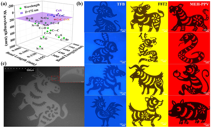
The mechanism behind this approach lies in the photon energy of 172 nm radiation (∼7.2 eV, 693.9 kJ/mol), which is sufficiently high to break most of the chemical bonds present in PSCs. As shown in Fig. 1a, this photon energy surpasses the dissociation energies of typical bonds in PSCs, making it highly effective for selective etching. This enables the decomposition of irradiated polymer regions without the need for photoresists, allowing for direct pattern transfer from photomasks (parameters shown in Fig. S1 in Supporting information) to PSC surfaces. To demonstrate the effectiveness of this technique, we successfully patterned emissive polymer semiconductor films deposited on transparent, flexible polyimide (PI) substrates. These films incorporated intricate designs, such as the twelve animals of the Chinese zodiac, as shown in Fig. 1b. The molecular structures of the emissive polymers, poly[(9,9-dioctylfluorenyl-2,7-diyl)-alt-(4,4′-(N-phenyl)-diphenylamine)] (TFB), poly[(9,9-dioctylfluorenyl-2,7-diyl)-alt-(2,2′-bithiophene)] (F8T2), and poly(2-methoxy,5-(2′-ethylhexyloxy)-1,4-phenylenevinylene) (MEH-PPV), are detailed in Fig. S2 (Supporting information). The resulting patterns exhibited clear, well-defined graphics, observable at specific excitation wavelengths. High-resolution scanning electron microscopy (SEM) images of the ox horn pattern (Fig. 1c) revealed sharp, well-defined edges with a resolution of ∼350 nm. Remarkably, the patterning quality achieved through 172 nm EVUL was comparable to that of commercial photolithography techniques.
Figure 1
Figure 1.
172 nm EVUL patterning of PSCs. (a) Relationship between the 172 nm EVUL photon energy and the dissociation energies of common chemical bonds in PSCs (with corresponding photon wavelengths). (b) Emissive polymers TFB, F8T2, and MEH-PPV patterned on a PI substrate using 172 nm EVUL. The corresponding excitation wavelengths were 254 nm for TFB, and 450 nm for F8T2 and MEH-PPV. (c) SEM images of cattle (scale bar: 50 µm). The inset shows an SEM image of the ox horn (scale bar: 5 µm).
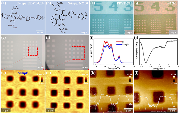
Building on the success of patterning irregular designs, we extended this technique to create well-defined molecular structures and square micro-array on representative p-type polymer PDVT-C10 (Fig. S3 in Supporting information) and n-type polymer N2200 films (Figs. 2a–d). These micro-patterns were precisely defined at feature sizes of 3, 4, and 5 µm, demonstrating the high precision and versatility of the 172 nm EVUL technique. The ability to achieve such fine feature sizes is particularly crucial for the developmenting high-density organic electronic devices, where maintaining pattern fidelity and resolution is essential. Optical transmission-mode images of the PDVT-C10 square array (3 µm and 4 µm features) on PI substrates are presented in Figs. 2e and f, providing clear visual confirmation of the uniformity and precision achieved through EVUL. High-resolution mapping scans of the highlighted regions in Figs. 2g and h further support the high pattern fidelity achieved, essential for ensuring the performance and stability of organic electronic devices at the micro-scale.
Figure 2
Figure 2.
High-resolution patterns prepared from P-type (PDVT-C10) and N-type (N2200) polymer semiconductors on PI by 172 nm EVUL etching. (a–d) Optical microscopy images of polymer semiconductors with corresponding molecular structure patterns and well-defined square array patterns. To enhance pattern distinction, optical microscopy images of (a) and (b) were stained with black and lilac for the etched and un-etched regions, respectively. (e, f) Optical transmission images of polymer semiconductor PDVT-C10 on a PI substrate, with patterns exhibiting resolutions of 3 and 4 µm, respectively. (g, h) Corresponding mapping scan images of the red inset regions, showing high pattern fidelity. (i) Micro-region transmission spectrum comparison between the etched (residual PI substrate) and un-etched regions. (j) The calculated absorption spectrum of the PDVT-C10 film, based on the results from the previous figures. (k, l) AFM images of micrometer-scale patterns derived from PDVT-C10-based film patterns. The patterns consist of square grooves of 3 and 4 µm, with the figures illustrating the height variation profiles.
Transmission spectra collected from both the patterned PDVT-C10 and bare PI substrate regions were clearly distinguishable, as shown in Figs. 2i and j. By dividing the PDVT-C10 spectrum by that of the PI substrate, we calculated the polymer transmittance spectra, revealing a characteristic absorption peak at approximately 1.45 eV. This result is consistent with previous studies on the optical properties of PDVT-C10 [34]. Additionally, atomic force microscopy (AFM) images of the 3 and 4 µm square arrays (Figs. 2k and l) confirmed that the patterned regions exhibited sharp, clean edges, validating the exceptional resolution and pattern definition provided by the 172 nm EVUL technique. Taken together, these results demonstrate the outstanding capability of the EVUL method for direct, high-resolution patterning of PSCs, while also underscoring its reproducibility and reliability for advancing organic electronics.
High-quality PTFT devices are essential for realizing circuit with low power consumption and high stability. To achieve this, we selected the near-amorphous polymer IDT-BT (the corresponding molecular structure of IDT-BT is shown in Fig. S4 in Supporting information) due to its favorable morphology, which promotes the uniform distribution of defects. This uniformity is crucial for maintaining stable and reproducible electronic performance across a wide range of operational conditions, ensuring consistent device performance and improving overall stability.
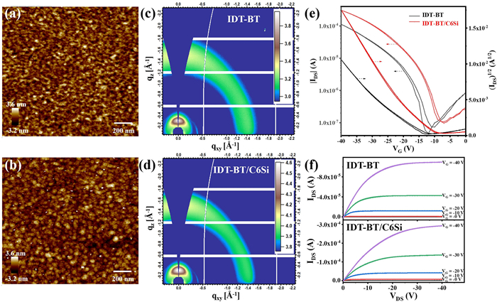
Furthermore, to enhance the charge transport properties of the IDT-BT polymer, we introduced doping by incorporating 1,6-bis(trichloromethylsilyl) hexane (C6Si). This modification significantly altered the micromorphology of the polymer film, as illustrated in Figs. 3a and b. The root mean square (RMS) roughness increased from 0.86 nm to 1.13 nm, and the grain size expanded, which was beneficial for improving carrier mobility. Despite these changes, the doped IDT-BT films remained near-amorphous across the entire scanning range, as confirmed by GIWAXS measurements (Figs. 3c and d, Fig. S5 and Table S1 in Supporting information). The slight narrowing of the diffraction peak at the (100) plane indicated an improvement in crystallization quality without disrupting the overall stacking structure.
Figure 3
Figure 3.
Comparison of the original and doped polymer IDT-BT films. Samples were used identical blend solutions as those used in devices. (a, b) AFM height images of IDT-BT and IDT-BT(C6Si)-based film. (c, d) Two-dimensional GIWAXS images of IDT-BT and IDT-BT(C6Si)-based film. (e, f) Transfer and output characteristics of IDT-BT and IDT-BT(C6Si)-based films (VG = −40 V, VDS = −40 V).
To evaluate the electrical impact of this doping, we fabricated PTFTs using both pristine and doped IDT-BT films. The typical transfer and output curves of the thin-film field-effect transistors (FETs) based on the original and doped IDT-BT are shown in Figs. 3e and f. As expected, doping significantly improved the device performance, nearly tripling the mobility. The maximum mobility of the IDT-BT thin film on a Corning glass substrate reached 0.42 cm2 V−1 s−1, while the doped IDT-BT reached 1.18 cm2 V−1 s−1. Additionally, PTFTs with doped IDT-BT exhibited a lower threshold voltage of approximately 8 V, compared to 12.5 V for devices using undoped IDT-BT films in the saturation regime. This improvement in both mobility and threshold voltage indicates that doping with C6Si effectively enhances the charge transfer properties and overall performance of the PTFTs, making it a promising approach for developing high-performance organic electronics.
For integrated circuit applications, lossless patterning is a prerequisite for efficient operation. Effective patterning techniques not only avoid damaging the polymer semiconductor but also help suppress off-state current, increase switching ratios, and improve fabrication yield. Importantly, leakage current differences between patterned and unpatterned devices strongly affect mobility calculations. Thus, reducing leakage current is vital for improving device performance, lowering power consumption, and enhancing operational stability. In this context, we successfully applied 172 nm EVUL etching to fabricate 360 PTFT array on Si/SiO2 substrates based on doped IDT-BT. As shown in Fig. S6 (Supporting information), the array adopted a bottom-gate, top-contact architecture on a 5 cm × 4.5 cm Si/SiO2 substrate treated with octadecyltrichlorosilane (OTS). Three PTFT devices were evenly distributed per square centimeter. The optical microscope image of a single device revealed well-defined edges, with the channel length and width of the Au electrodes measured at 5 and 500 µm, respectively. Device-level performance before and after etching (Fig. S7 in Supporting information) showed improvements: Mobility increased from 0.66 cm2 V−1 s−1 to 0.72 cm2 V−1 s−1 (VG = −20 V, VDS = −20 V), while off-state current dropped by three orders of magnitude (from 10−9 A to 10−12 A). These results suggest that EVUL etching effectively reduces leakage and increases switching ratios in PTFT array. In addition, we selected the 1st, 6th, 11th, and 16th devices from each column, totaling 72 devices, and performed statistical analysis on their performance metrics, including mobility, threshold voltage, and Ion/Ioff ratio (Fig. S8 in Supporting information). These statistics confirm the method’s reproducibility.
TFTs have long been central to display technology since the first demonstration of a-Si TFT-driven liquid crystal displays (LCDs) in 1981 [35]. With the growing demand for high-resolution and flexible displays, polymer semiconductor-based PTFTs have emerged as promising candidates due to their inherent advantages, and their performance has now reached the threshold of practical application. Here, we demonstrate this potential by fabricating PTFT-organic light-emitting diode (OLED) active-matrix circuit on flexible polyethylene terephthalate (PET) substrates using 172 nm EVUL etching.
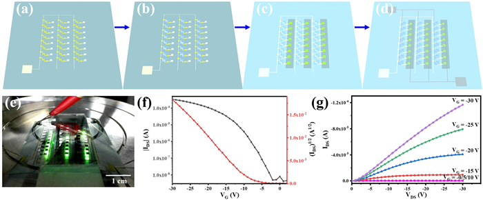
As shown in Figs. 4a–d, a top-gate, bottom-contact configuration was selected to enhance device stability. Au was first evaporated to form the source and drain electrodes of the PTFTs, the OLED anode, and interconnects. A doped IDT-BT film was then spin-coated and patterned by 172 nm EVUL etching, followed by deposition of a polymethyl methacrylate (PMMA) dielectric layer. This compact PMMA film not only served as a gate dielectric but also acted as a protective encapsulation layer, preventing the OLED from being influenced by the PTFT gate field. After selectively removing PMMA over the OLED anode by O2 plasma etching, OLED layers were deposited. Finally, PTFT-OLED active circuit were fabricated on a 5 × 5 cm2 PET substrate with green emissive dyes (Fig. 4e), exhibiting bright and clearly visible emission even in the bottom-emitting configuration (Fig. S9 in Supporting information demonstrating active-matrix circuit on a glass substrate). Electrical characterization further confirmed the uniform driving capability of the doped IDT-BT PTFTs (Figs. 4f and g). Under a constant gate and drain voltage of –30 V, the PTFTs switched on, delivering a current density of ∼3.4 × 10⁻⁴ A/cm2 to drive the OLEDs, the resulting PLED achieved a maximum luminance of 10964 cd/m2, with a current efficiency (CE) of 13.13 cd/A (Fig. S10 in Supporting information). After 100 bending cycles, the on-state current decreased to ∼1.05 × 10⁻⁴ A (Fig. S11 in Supporting information). These results collectively demonstrate the feasibility of EVUL-patterned PTFTs in flexible, large-area active-matrix OLED circuit and underscore their potential for next-generation organic electronics.
Figure 4
Figure 4.
The 172 nm EVUL etching as an effective strategy to realize electronic circuit. Process diagrams for PTFT active-matrix circuit: (a) Evaporation of Au to form patterns for the OLED anode, source and drain electrodes for the PTFTs, and source bonding. (b) Deposition of doped IDT-BT film followed by 172 nm EVUL patterning. (c) O2 plasma etching to remove PMMA over the OLED anode, followed by OLED evaporation. (d) Bonding of OLEDs and PTFTs. (e) Photo image of PTFT active-matrix circuit on a flexible PET substrate. (f, g) Transfer and output curves of the PTFT-OLED active-matrix (VG = −30 V, VDS = −30 V), showing the performance characteristics of the circuit.
In conclusion, 172 nm EVUL etching offers a versatile, high-resolution patterning technique for polymer semiconductors. This method achieves resolutions as fine as ∼350 nm, facilitates the fabrication of a 360-device PTFT array with a four-order-of-magnitude reduction in leakage current, and supports integration into active PTFT-OLED circuits with enhanced brightness. Taken together, these findings highlight the potential of EVUL etching as a scalable and reliable solution for advancing polymer-based optoelectronics, particularly in flexible integrated circuits, wearable devices, and next-generation displays.
The authors declare that they have no known competing financial interests or personal relationships that could have appeared to influence the work reported in this paper.
Acknowledgments
This work was financially supported by the National Key R&D Program of China (No. 2023YFB3609000), the National Natural Science Foundation of China (Nos. T2441002, U24A20137, U22A6002, 22525506), the Strategic Priority Research Program of CAS (No. XDB0520101), the CAS Project for Young Scientists in Basic Research (No. YSBR-053). X-ray data was acquired at beamlines 7.3.3 and 11.0.1.2 at the Advanced Light Source, which is supported by the Director, Office of Science, Office of Basic Energy Sciences, of the U.S. Department of Energy under Contract No. DE-AC02-05CH11231. The authors thank Chenhui Zhu at beamline 7.3.3, and Cheng Wang at beamline 11.0.1.2 for assistance with data acquisition.
Supplementary materials
Supplementary material associated with this article can be found, in the online version, at doi:10.1016/j.cclet.2025.112323.
H.J. Chen, Y.L. Guo, G. Yu, et al., Adv. Mater. 24 (2012) 4618–4622. doi: 10.1002/adma.201201318
[35]
A.J. Snell, K.D. Mackenzie, W.E. Spear, et al., Appl. Phys. Lett. 24 (1981) 357–362.
Figure 1
172 nm EVUL patterning of PSCs. (a) Relationship between the 172 nm EVUL photon energy and the dissociation energies of common chemical bonds in PSCs (with corresponding photon wavelengths). (b) Emissive polymers TFB, F8T2, and MEH-PPV patterned on a PI substrate using 172 nm EVUL. The corresponding excitation wavelengths were 254 nm for TFB, and 450 nm for F8T2 and MEH-PPV. (c) SEM images of cattle (scale bar: 50 µm). The inset shows an SEM image of the ox horn (scale bar: 5 µm).
Figure 2
High-resolution patterns prepared from P-type (PDVT-C10) and N-type (N2200) polymer semiconductors on PI by 172 nm EVUL etching. (a–d) Optical microscopy images of polymer semiconductors with corresponding molecular structure patterns and well-defined square array patterns. To enhance pattern distinction, optical microscopy images of (a) and (b) were stained with black and lilac for the etched and un-etched regions, respectively. (e, f) Optical transmission images of polymer semiconductor PDVT-C10 on a PI substrate, with patterns exhibiting resolutions of 3 and 4 µm, respectively. (g, h) Corresponding mapping scan images of the red inset regions, showing high pattern fidelity. (i) Micro-region transmission spectrum comparison between the etched (residual PI substrate) and un-etched regions. (j) The calculated absorption spectrum of the PDVT-C10 film, based on the results from the previous figures. (k, l) AFM images of micrometer-scale patterns derived from PDVT-C10-based film patterns. The patterns consist of square grooves of 3 and 4 µm, with the figures illustrating the height variation profiles.
Figure 3
Comparison of the original and doped polymer IDT-BT films. Samples were used identical blend solutions as those used in devices. (a, b) AFM height images of IDT-BT and IDT-BT(C6Si)-based film. (c, d) Two-dimensional GIWAXS images of IDT-BT and IDT-BT(C6Si)-based film. (e, f) Transfer and output characteristics of IDT-BT and IDT-BT(C6Si)-based films (VG = −40 V, VDS = −40 V).
Figure 4
The 172 nm EVUL etching as an effective strategy to realize electronic circuit. Process diagrams for PTFT active-matrix circuit: (a) Evaporation of Au to form patterns for the OLED anode, source and drain electrodes for the PTFTs, and source bonding. (b) Deposition of doped IDT-BT film followed by 172 nm EVUL patterning. (c) O2 plasma etching to remove PMMA over the OLED anode, followed by OLED evaporation. (d) Bonding of OLEDs and PTFTs. (e) Photo image of PTFT active-matrix circuit on a flexible PET substrate. (f, g) Transfer and output curves of the PTFT-OLED active-matrix (VG = −30 V, VDS = −30 V), showing the performance characteristics of the circuit.


 DownLoad:

 下载:


 下载:

