Citation:
Kangyuan Xie, Shen Chen, Zhi Ye, Min Chen, Hanying Li. Unveiling the intrinsic dielectric constant of form Ⅲ iPB-1 single crystals[J]. Chinese Chemical Letters,
2026, 37(10): 112165.
doi:
10.1016/j.cclet.2025.112165
Unveiling the intrinsic dielectric constant of form Ⅲ iPB-1 single crystals
English
Unveiling the intrinsic dielectric constant of form Ⅲ iPB-1 single crystals
MOE Key Laboratory of Macromolecular Synthesis and Functionalization, International Research Center for X Polymers, Shanxi-Zheda Institute of Advanced Materials and Chemical Engineering, Department of Polymer Science and Engineering, Zhejiang University, Hangzhou 310027, China
Received Date:
04 November 2025 Accepted Date:
24 November 2025 Revised Date:
23 November 2025 Available Online:
15 October 2026
Abstract:
Polymer lamellar single crystals (PLSCs), the fundamental crystalline units of semicrystalline polymers, are ideal model systems to probe intrinsic structure-property relationships of polymer dielectrics. However, the reliable preparation and characterization of PLSCs remain challenging. Here, using a controlled solvent evaporation method, large-area isotactic poly(1-butene) (iPB-1) single crystals with lateral dimension spanning several hundred micrometers were directly grown on conductive substrates. This, in turn, enables straightforward fabrication of metal–insulator–metal (MIM) capacitors, and facilitates the subsequent determination of the dielectric constant for form Ⅲ iPB-1 single crystals with a remarkably low value of 1.82 ± 0.05. This low value is attributed to suppressed chain-segmental motion and low molecular packing density of form Ⅲ crystal phase. This study provides a model framework for quantifying the intrinsic dielectric performance of crystalline phase in semicrystalline polymer systems and highlighting the importance of crystal structure in determining the macroscopic behavior of polymeric dielectrics.
Under an external electric field, the polarization response within a material determines its dielectric constant, which is one of the crucial performance metrics for dielectrics [1–4]. For polymers, their complex hierarchical structures lead to diverse and often unpredictable polarization behaviors [5–7]. In particular, semicrystalline polymers are typically composed of both crystalline and amorphous regions, which exhibit intrinsically different responses to external electric fields [8–10]. In the crystalline domains, molecular chains are highly ordered and constrained within the lattice, and dielectric constant is limited by constrained dipole orientation [11–16]. In contrast, in the disordered regions, the chain-segmental motion is enabled, enhancing polarization [17–19]. This disparity between the two phases not only leads to pronounced frequency-dependent dielectric responses but also makes the dielectric performance of polymers highly sensitive to materials batch, processing methods, and post-treatment conditions [8,9,20–24].
Therefore, effectively decoupling the dielectric behaviors of crystalline and amorphous structures within such hierarchical systems and elucidating their respective contributions to the macroscopic dielectric properties constitute a key scientific challenge in understanding the origins and even the limits of performance in polymer dielectric materials. Generally, this disparity was often assessed through the frequency-dependent differences in dielectric constants between crystalline and amorphous phases, where the crystalline component was usually approximated using the value measured at high frequencies or low temperatures [19,25,26]. While these qualitative insights provide empirical guidance, the evolution from qualitative observation to quantitative understanding of the origin of the materials properties has long been a fundamental driving force behind the advancement of materials science. This need has become more pronounced today, as the development of materials has been greatly accelerated by the application of data-driven and AI-assisted approaches, where physically interpretable and quantitatively reliable parameters as meaningful input for predictive modeling is required.
To address these challenges, polymer lamellar single crystals (PLSCs), serving as the basic building blocks of semicrystalline polymers [27–29], provide an ideal model system for isolating and characterizing the intrinsic dielectric response of the crystalline region.
The availability of large-area polymer single crystals is paramount to probing their intrinsic dielectric characteristics. However, the realization of these large-sized polymer single crystals has remained a persistent challenge. Although “self-seeding” crystallization technique enabled the production of lamellar polymer crystals with dimensions reaching tens of micrometers [30,31], sometimes with the largest size of one hundred micrometer through precise manipulation of crystallization parameters [14], these crystals were typically too small for common dielectric characterization strategies. Furthermore, this method usually yields polymer crystals dispersed in solution, requiring additional transfer steps for device fabrication, which often causes damage to the ultrathin polymer crystals and complicates the vertical metal–insulator–metal (MIM) device construction. To address these challenges, in the present work, we developed a controlled solvent evaporation method that enables the direct deposition of large-area PLSCs onto the substrate.
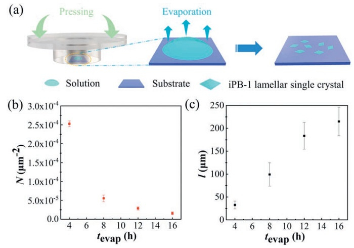
Fundamentally, achieving large-area single crystals necessitates refined control of both nucleation and crystal growth kinetics. The conventional “self-seeding” method relies on precise temperature control to modulate the degree of supercooling, determining the thermodynamic driving force for crystallization and thereby influencing both nucleation and crystal growth processes. Solvent evaporation crystallization, in contrast, modulates supersaturation through leveraging increasing solute concentration driven by controlled solvent evaporation [32–35]. Then, the concentration profile of the crystal growth front can be precisely tuned by the evaporation rates. To achieve precise control over solvent evaporation, we designed a custom solution evaporation apparatus providing precise control over solvent evaporation (Fig. 1a). The chamber atmosphere can be modulated via a variable-force lid, applying greater force enhances the chamber’s sealing and thereby suppresses the evaporation rate.
Figure 1
Figure 1.
Preparation of single crystals via controlled solvent evaporation method. (a) Schematic illustration of the controlled solvent evaporation crystallization. (b) Crystal number density (N) and (c) average lateral size (measured along the long axis of lozenge-shaped crystals) as a function of total evaporation time (tevap), respectively (statistics from 5 samples comprising 40 crystals in total at each tevap, and data are presented as mean ± standard deviation (SD)).
Fig. S1 (Supporting information) summarized isotactic poly(1-butene) (iPB-1) lamellar single crystal morphologies at different total evaporation time (tevap), with corresponding crystal number density (N) and average lateral size (l) data presented in Figs. 1b and c respectively. Following solvent evaporation, the substrate was consistently covered in lozenge-shaped crystals. And the increasing tevap from 4 h to 12 h resulted in N gradually decreasing from 2.5 × 10⁻⁴ µm−2 to 2.9 × 10⁻⁵ µm−2, while average l (long axis of lozenge-shaped crystals) increased from 32 µm to 183 µm, demonstrating that slower evaporation tends to reduce nucleation density and yield larger crystals.
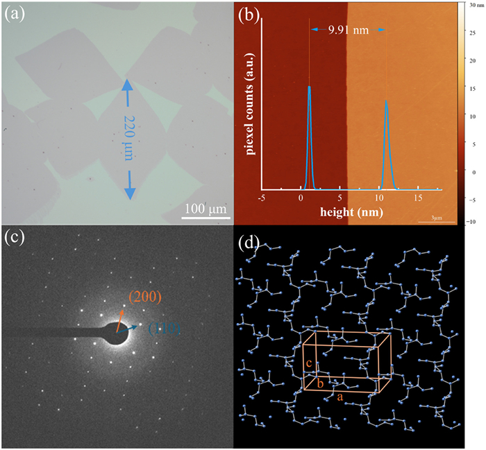
Although further reducing the evaporation rate to achieve a tevap of 16 h resulted in a larger average crystal size exceeding 200 µm, the prolonged crystallization time promotes competition between lateral growth and the formation of stacked layers [32]. This multi-layer growth (Fig. S2 in Supporting information), along with the presence of screw dislocations, is not expected for the device fabrication and dielectric performance measurement. Therefore, to achieve both large size and uniformity, we optimized the evaporation time to 12 h, which yielded iPB-1 PLSCs with a maximum lateral size over 200 µm (Fig. 2a). Atomic force microscopy (AFM) revealed that the large iPB-1 PLSCs possessed a uniform thickness of 9.91 nm (Fig. 2b), with an average thickness of 10.15 ± 0.31 nm based on measurements of 10 crystals (Fig. S3 in Supporting information), consistent with previously reported values [36]. As shown in Fig. 2c, the crystallographic features of the obtained crystals were further investigated using selected area electron diffraction (SAED) analysis. The resulting SAED patterns were consistent with the [001] zone axis diffraction pattern of the form Ⅲ crystalline phase of iPB-1, characterized by a 4/1 helical conformation packed in an orthorhombic lattice (Fig. 2d) [37,38]. The SAED data also indicated that the c-axis (corresponding to the polymer chain direction) of these crystals was oriented perpendicular to the substrate. Form Ⅲ is a special metastable phase exhibiting a looser packed structure than the most common form Ⅰ, yet it is significantly more stable than the other metastable phase of form Ⅱ [39–41].
Figure 2
Figure 2.
Morphology and structure of iPB-1 PLSCs. (a) Optical microscopy (OM) image of iPB-1 PLSCs exhibiting optimized lateral size and uniformity. (b) Atomic force microscopy (AFM) topographic image of an iPB-1 PLSC. Inset: Height profile obtained from the AFM scan, used for accurate determination of the iPB-1 PLSC thickness. (c) Selected area electron diffraction (SAED) pattern obtained from an iPB-1 PLSC. (d) Crystal structure of iPB-1 form Ⅲ crystals.
The dielectric constant (k) can be reliably determined through capacitance of vertical MIM parallel-plate capacitors. To realize MIM devices, we need to fabricate electrodes on both the top and bottom surfaces of the lamellar crystal, which was challenging for fragile, small-sized crystals (<100 µm) suspended in solvent that obtained through conventional “self-seeding” methods. Here, within controlled solvent evaporation method, large-area iPB-1 single crystals with lateral dimensions spanning several hundred micrometers were obtained. Furthermore, this controlled evaporation approach enabled direct deposition of the as-grown single crystals onto conductive substrates, thereby simplifying the fabrication of MIM capacitors.
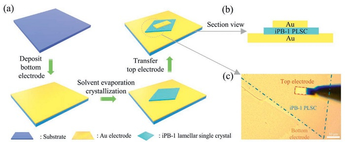
As shown in Fig. 3a, the MIM vertical parallel-plate capacitors were fabricated by first depositing a uniform 25 nm layer of gold onto silicon wafers via thermal vapor deposition, which served as the conductive bottom electrode. Subsequently, iPB-1 PLSCs were grown directly on this gold electrode using a controlled solvent evaporation method. This in-situ growth approach minimized the risk of transfer-induced damage and ensured intimate interfacial contact. The large iPB-1 PLSCs further enabled facile capacitor fabrication via direct transfer of gold top electrodes onto selected regions.
Figure 3
Figure 3.
Fabrication and structure of MIM capacitor devices incorporating iPB-1 PLSCs as the dielectric layer. (a) Schematic illustration of the MIM capacitor device fabrication process, involving direct growth of iPB-1 PLSCs onto the bottom electrode and subsequent transfer of the top electrode. (b) Cross-sectional schematic of the fabricated MIM capacitor device. (c) OM image of a representative iPB-1 PLSC-based MIM capacitor device.
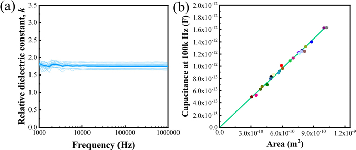
And then the dielectric constant k was determined by analyzing capacitor parameters from impedance measurements and applying the equation: k=Ct/ε0A, where C denotes the capacitance, t is the thickness of the dielectric layer, εn is the vacuum permittivity, and A is the effective device area (i.e., the overlap area between the top and bottom electrodes). The extracted dielectric constant versus frequency from 25 capacitors were plotted in Fig. 4a. The dielectric constant k is approximately constant over a wide range of frequencies and has an average value of 1.82 ± 0.05 at 100 kHz. This astonishing value is much lower than the reported values of 2.10–2.53 for iPB-1 based materials [26,42–44] and is also lower than most dense polymer dielectrics with a dielectric constant exceeding 2.0 [7,10,45–47]. To mitigate potential errors in dielectric constant determination arising from the small device area, we performed capacitance measurements on a series of devices with varying electrode areas (Figs. S4 and S5 in Supporting information) [48]. As shown in Fig. 4b, the proportional relationship between capacitance and area indicates that the k value we derived is independent of device area and unaffected by area measurement errors. According to slope of C-A, k was determined with the value of 1.79, consistent with the average value of 1.82 ± 0.05, confirming the validity of our method and the derived k value of 1.82 ± 0.05 as the intrinsic dielectric constant of the iPB-1 PLSCs.
Figure 4
Figure 4.
The dielectric constant of iPB-1 PLSCs. (a) Relative dielectric k as a function of frequency for iPB-1 PLSCs. The thick blue line represents the average dielectric constant across 25 devices. (b) Measured capacitance of iPB-1 PLSC-based MIM capacitors plotted as a function of device area. Each data point represents a device, with a total of 24 devices fabricated from 8 crystals. The device area was controlled by adjusting the contact between the electrode and the crystal during the transfer process.
The dielectric constant quantifies a material’s ability to be polarized by an electric field. According to the Clausius-Mossotti relationship [49], the dielectric constant k of nonpolar dielectrics can be expressed as: (k−1)/(k+2)=Nα/3ε0, where α is the electronic polarizability, N is the number of molecules per unit volume, and εn is the vacuum permittivity. The Clausius-Mossotti equation dictates that k decreases with decreasing polarizability (α) or the number of molecules per unit volume (N). As discussed previously, the highly ordered and densely packed polymer chains within the crystal lattice of PLSCs can significantly suppress chain segment motion and dipole orientation, reducing the dielectric’s polarizability (α) and resulting in a lower k. Furthermore, the unique crystal structure and molecular packing of form Ⅲ iPB-1 also contribute to its low k. Form Ⅲ, a metastable phase with a more loosely packed arrangement of polymer chains than the commonly observed form Ⅰ, exhibits a Kitaigorodskii packing coefficient [50] of 0.64 (compared to 0.68 for form Ⅰ) [37], resulting in a corresponding density of 0.894 g/cm3, approaching that of amorphous iPB-1 (0.868 g/cm3) and significantly lower than form Ⅰ crystals (0.950 g/cm3) [51]. This difference in packing coefficients and densities suggests a higher void fraction within form Ⅲ crystals compared to form Ⅰ, leading to a lower N and further reducing the dielectric constant. The synergistic effect of decreased polarizability and reduced molecular density therefore results in the characteristically low dielectric constant observed in form Ⅲ iPB-1 lamellar single crystals.
In summary, with the precise control over the solvent evaporation rate, we have successfully implemented a controlled solvent evaporation method to achieve the growth of large-area (over 200 µm lateral dimension), high-quality form Ⅲ iPB-1 PLSCs directly onto conductive substrates, which then simplified fabrication of MIM capacitors. Based on these MIM capacitors, the surprisingly low dielectric constant of 1.82 ± 0.05 at 100 kHz for the form Ⅲ iPB-1 single crystals was revealed. This exceptionally low value was attributed to a synergistic effect resulting from reduced molecular packing density of the special form Ⅲ polymorph and suppressed chain segment motion in the highly ordered crystalline structure. This work not only demonstrates a robust and efficient method for directly probing these intrinsic structure-property relationships via solvent evaporation crystallization and facile MIM capacitor fabrication but also indicates the critical role of crystal structure in governing the dielectric properties of semicrystalline polymers. These findings presented here holds great promise for the preparation and characterization of other polymeric single crystals, providing a valuable tool for mapping the relationship between crystal structure and dielectric properties in a wide variety of semicrystalline polymer dielectrics.
The authors declare that they have no known competing financial interests or personal relationships that could have appeared to influence the work reported in this paper.
Acknowledgments
This work was supported by the National Natural Science Foundation of China (Nos. U23A20592, 52394274), and the Fundamental Research Funds for the Central Universities (No. 226-2025-00031).
Supplementary materials
Supplementary material associated with this article can be found, in the online version, at doi:10.1016/j.cclet.2025.112165.
J.G. Speight, Dielectric constant, in: J.G. Speight (Ed.), Rules of Thumb for Petroleum Engineers, 1st ed, John Wiley & Sons, Hoboken, 2017, p. 229.
[5]
C.A. Buehler, J. Electrochem. Soc. 115 (1968) 271C. doi: 10.1149/1.2411454
[6]
G. Williams, Dielectric properties of polymers, in: R.W. Cahn, P. Haasen, E.J. Kramer (Eds.), Materials Science and Technology„ 1st ed, John Wiley & Sons, Weinheim, 2006, pp. 471–528.
B. Lotz, J.C. Wittmann, Structure of polymer single crystals, in: R.W. Cahn, P. Haasen, E.J. Kramer (Eds.), Materials Science and Technology, 1st ed., John Wiley & Sons, Weinheim, 2006, pp. 79–151.
[28]
K.L. Xu, B.H. Guo, R. Reiter, et al., Chin. Chem. Lett. 26 (2015) 1105–1108. doi: 10.1016/j.cclet.2015.06.002
A. Kitaigorodsky, Molecular Crystals and Molecules, Elsevier, 2012.
[51]
D. Maring, B. Meurer, G. Weill, J. Polym. Sci. Part B 33 (1995) 1235–1247.
Figure 1
Preparation of single crystals via controlled solvent evaporation method. (a) Schematic illustration of the controlled solvent evaporation crystallization. (b) Crystal number density (N) and (c) average lateral size (measured along the long axis of lozenge-shaped crystals) as a function of total evaporation time (tevap), respectively (statistics from 5 samples comprising 40 crystals in total at each tevap, and data are presented as mean ± standard deviation (SD)).
Figure 2
Morphology and structure of iPB-1 PLSCs. (a) Optical microscopy (OM) image of iPB-1 PLSCs exhibiting optimized lateral size and uniformity. (b) Atomic force microscopy (AFM) topographic image of an iPB-1 PLSC. Inset: Height profile obtained from the AFM scan, used for accurate determination of the iPB-1 PLSC thickness. (c) Selected area electron diffraction (SAED) pattern obtained from an iPB-1 PLSC. (d) Crystal structure of iPB-1 form Ⅲ crystals.
Figure 3
Fabrication and structure of MIM capacitor devices incorporating iPB-1 PLSCs as the dielectric layer. (a) Schematic illustration of the MIM capacitor device fabrication process, involving direct growth of iPB-1 PLSCs onto the bottom electrode and subsequent transfer of the top electrode. (b) Cross-sectional schematic of the fabricated MIM capacitor device. (c) OM image of a representative iPB-1 PLSC-based MIM capacitor device.
Figure 4
The dielectric constant of iPB-1 PLSCs. (a) Relative dielectric k as a function of frequency for iPB-1 PLSCs. The thick blue line represents the average dielectric constant across 25 devices. (b) Measured capacitance of iPB-1 PLSC-based MIM capacitors plotted as a function of device area. Each data point represents a device, with a total of 24 devices fabricated from 8 crystals. The device area was controlled by adjusting the contact between the electrode and the crystal during the transfer process.


 DownLoad:

 下载:
下载:


 下载:
下载:

