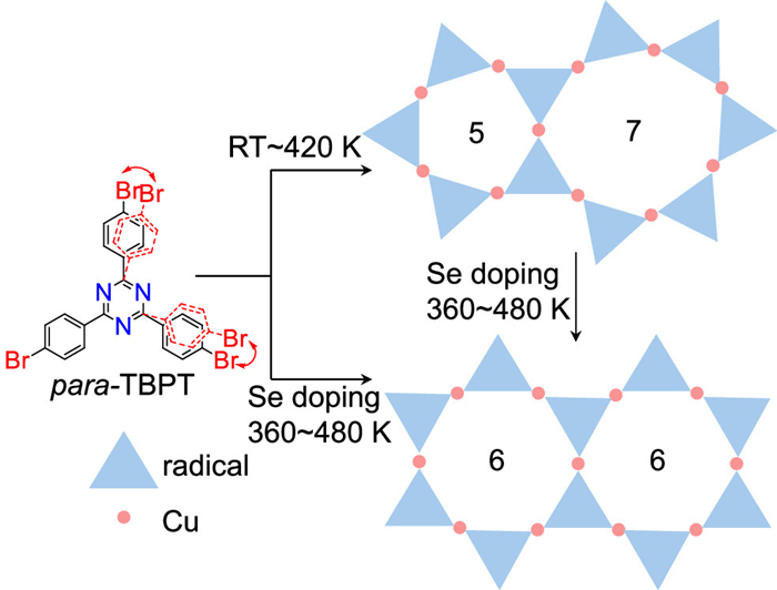
Scheme 1.
Structural diagram and reaction pathway. Reaction pathway of pTBPT on Cu (111) toward OMs with different membered rings and ordered hexagonal OMs after selenium doping.
Disorder–order transition of two-dimensional molecular networks by selenium doping
Liangliang Cai , Xinyi Zhang , Jiayi Lu , Juan Xiang , Qiang Sun , Andrew T.S. Wee

At the nanometer scale, geometrical dimensions and topologies are inherently linked to their electronic properties, with the exciting opportunity to engineer the latter through precise structural control [1–6]. Nanostructures based on the honeycomb lattice have emerged as a versatile platform in the development of energy technologies, quantum computing, and nanoscale sensing [5,7,8]. Their unique electronic properties, including the massless Dirac fermions and topologically protected states, have attracted significant interest for a wide range of applications [9,10]. Achieving a perfect honeycomb network with large-scale order for systems is technically promising, while still remains challenging. This is especially so at the atomic scale, where defects and disordering can dramatically compromise their performance. Using a precursor monomer with enhanced structural rigidity would possibly result in a more uniform network [11–16]. Different growth parameters (evaporation flux, type of substrate, and temperature) have been studied to explore the optimum experimental conditions required for the formation of a polymer with fewer defects [17–22]. However, for the general tripod monomers without rigidity, the intrinsic topological defects cannot be mitigated by different preparation parameters. The conformational flexibility of the precursor skeleton, which accommodates deformation of precursor monomers with limited tension, prevents the formation of a complete ordered network.
To address this issue, we adopted the general tripod precursor 2,4,6-tris(4-bromophenyl)-1,3,5-triazine (pTBPT), in which the triazine ring is equipped with three para-bromophenyl groups. As shown in Scheme 1, the 3-equiv. terminal bromophenyl units (marked in red in Scheme 1) can bend from their ideal positions (black) through the flexibility of C–C σ bonds between two neighboring phenyl units, reducing the 3-fold molecular symmetry. Consequently, polygons of different edges (4, 5, 7, 8, etc.) were observed after C–Cu–C metal organic frameworks (MOFs) fabrication on Cu (111) at room temperature (RT) to 420 K, in addition to hexagons as the ideal structural motif. These intrinsic topological defects could not be eliminated through thermal treatments (deposition on cold substrate followed by annealing or deposition on hot substrate), because polygons with different numbers of edges exhibit similar enthalpy values (Fig. S1 in Supporting information).
In our previous work, selenium (Se) doping has been demonstrated to achieve the topology selectivity of a conformationally flexible precursor [23], and this topic is also important in view of the increased interest in selenides. Therein, we have investigated the low coverage (~0.015 monolayer, ML) Se doping with pTBPT on Cu (111) and achieved the hexagonal organometallic (OM) nanostructure uniformity. The difference between the previous mTBPT and current pTBPT originates from that the former is bromine functionalized in the meta-sites and the latter in para-sites. Thus mTBPT has conformers with Cs and C3h symmetries by the rotation of the m-bromophenyl groups around the C–C σ-bonds to the central triazine ring, and right-handed and left-handed chirality upon two-dimensional (2D) confinement. However, pTBPT does not have these conformers and represents a much simpler and more general tripod precursor so that we can study the generality of the Se doping strategy. The significant improvement of the honeycomb network confirms the structural homogeneity, so that a sub-monolayer ordered 2D MOF is achieved by co-deposited pTBPT and Se at 360-480 K. The deposition sequence of pTBPT and Se does not make any difference owing to the reversibility of the MOF structure. In addition, the disordered network composed of different polygons can be transformed to the ordered hexagonal network by ~0.015 ML Se doping at 360-480 K. Annealing for enough time makes sure of the transformation to the ordered phase from a kinetic point of view. By high-resolution scanning tunneling microscopy/spectroscopy (STM/STS), we have explored the disorder−order transition of 2D molecular networks through Se doping on Cu (111). A persistent homology (PH) method is resorted to quantify the disorder−order level of our patterns. Density functional theory (DFT) calculations further reveal the regulation of energy diagrams in the absence or presence of Se and explain the transformation from the random phase to the ordered 2D MOF.
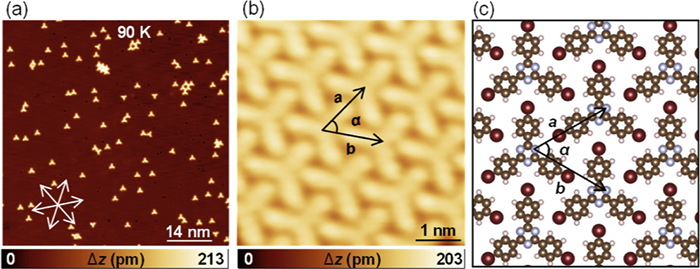
Deposition of sub-monolayer amounts of pTBPT on Cu (111) held at 90 K results in the formation of isolated monomers and self-assembled domains including compact phase and coexisting porous networks as illustrated in Fig. 1a. The close-up STM measurements in Figs. 1b and c reveal that the compact domains are stabilized by typical C–H···Br hydrogen bonding and Br···N halogen bonds [24]. The interaction region indicator (IRI) analysis on the finite dimer moiety was also performed to investigate the intermolecular interactions between two monomers in the compact phase [25]. As illustrated in the IRI isosurface (Fig. S2 in Supporting information), both covalent bond and weak interaction regions are revealed by the blue and green isosurfaces, respectively, according to the standard coloring method. This thus demonstrates that the C–H···Br hydrogen bonds, together with the Br···N halogen bond, are driving forces for the compact phase. The DFT relaxed model shown in Fig. 1c for the close-packed self-assembled phase indicates the lattice parameters of a = b = 1.34 nm and α = 120°, which agrees nicely with the measured values of a = b = 1.33 ± 0.05 nm and α = 120° ± 2°. As shown in Fig. S3 (Supporting information), the porous network is formed by intact pTBPT with characteristic C–Br···Br halogen bonding, featuring a rhombic unit cell with lattice parameters a1 = b1 = 1.68 ± 0.05 nm and α1 = 120° ± 2°, in good agreement with the theoretical prediction of a1 = b1 = 1.66 nm and α1 = 120°. Left- and right-handed homochiral domains of the porous networks are observed, which are unambiguously identified based on the characteristic halogen bond forming nodes (Fig. S3). The terminal Br groups form halogen bonds leading to a trimeric X3-synthon [26,27] with a typical Br···Br distance of about 0.4 nm [28–31].
After annealing the sample to 360 K overnight, disordered networks were observed as depicted in Fig. 2a. Upon closer inspection in Fig. 2b, the pTBPT precursor was fully debrominated and disordered OM networks were composed of linked monomers forming polygons mainly with between 4 and 8 edges. We correspond each molecule to one vertex, and the equivalent diameter (Eq. D) is calculated with the formula Eq.
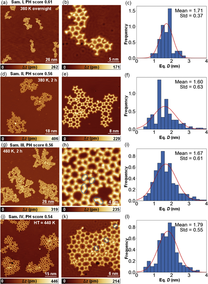
Testing different preparation parameters made it possible to determine the optimum experimental conditions required for the formation of networks with few defects. Different thermal treatments were studied, including deposition of pTBPT followed by annealing at 380 K (Sam. Ⅱ, Figs. 2d-f), and 460 K (Sam. Ⅲ, Figs. 2g-i), respectively. The samples were annealed with sufficient time of 2 h. Additionally, deposition of pTBPT on hot Cu (111) substrate maintained at 440 K was also examined from a kinetic perspective (Sam. Ⅳ, Figs. 2j-l). It is hard to discern improvement in network quality with annealing at 380 K (Figs. 2d and e). At higher temperatures around 460 K, demetallation occurred, with covalently interlinked moieties highlighted by blue ellipses in Figs. 2h and k. The disordered network samples exhibit broad distributions of equivalent diameters with standard deviation ranging from 0.37 to 0.63 (Figs. 2c, f, i, and l, the right column of Fig. 2). These broad distributions are attributed to the intrinsic flexibility of the molecular backbone structure. This critical result, combined with the observed high reaction yield, indicates that the system reaches equilibrium under the given conditions, and the presence of polygonal defects in the networks is inevitable.
To further quantify the degree of order in the molecular networks, we employed the persistent homology (PH) method [32,33]. Persistent diagrams were generated from STM topographic images to track the evolution of the pores in the molecular networks. The binarized STM image is illustrated in Fig. S4 (Supporting information), with additional statistical details provided in Fig. S5 (Supporting information). PH scores were computed based on the persistent diagrams, yielding a numerical metric to evaluate the regularity of the network. Initially developed for assessing the quality of surface-supported covalent networks, the principle of the PH method is also applicable to evaluating the degree of order in metal-organic networks. A score of 1 would be achieved for a perfectly regular network. As displayed in Fig. 2, the PH scores of the disordered networks range from 0.54 to 0.61. No further improvement was observed at higher temperatures (Sam. Ⅱ and Ⅲ). On the contrary, a slight decrease of PH score is noted owing to the demetallation process and the coexistence of organometallic and covalent structures. A different growth condition (deposition of pTBPT on hot Cu (111) substrate held at 440 K) was investigated. The rationale for this approach is that under that condition the networks may grow through the addition of monomers which are expected to have a much higher surface mobility. However, this approach did not yield significant improvements either. The PH score of Sam. Ⅳ equals to 0.54, which is very close to those of Sam. Ⅰ, Ⅱ and Ⅲ.
To make it simple, we discuss the major MOF structures here. The high defect density can be attributed to the energy necessary for wiggling the trigonal lobes of the pTBPT precursor. Due to the threefold symmetry of pTBPT, a hexagonal ring comprising six monomers yields the lowest-energy geometry (Fig. S1) as all newly formed links exhibited an ideal bonding angle of 180°. All other polygons experience slightly higher stress due to distortion of the monomer. Each bond between two phenyl lobes of a monomer in the polygon deviates from its optimal equilibrium angle on average by Δα = 60°(6 − N)/(3N) [18], where N denotes the number of molecules in the ring. The change Δα is small and accounts to 10°, 4°, 0°, −2.9°, and −5° for tetragon, pentagon, hexagon, heptagon, and octagon, respectively, yielding only a small additional energy contribution. This small deviation from the equilibrium geometry is responsible for the high number of polygons different from hexagons. Since linking of free radicals is virtually barrier free and only diffusion limited, kinetic effects can lead to suboptimal binding geometries where the binding angle deviates from 180°. This results in a reduced structural order and high defect densities. On the other hand, the flexibility of organometallic interlinking in the position of Cu adatoms accounts for both the small additional energy contribution and the frequent occurrence of polygons different from hexagons. As a result, the intrinsic topological defects persist regardless of different thermal treatments.
To address this issue, we turn to the doping effect drawing on literature regarding the regulation of metal or ion doping in on-surface 2D networks [34,35], particularly our previous study of Se doping, which has been demonstrated to achieve the topology selectivity of a conformationally flexible precursor mTBPT [23]. In this study, we investigated the low coverage (0.015 ML) Se doping with 0.28 ML pTBPT on Cu (111) and achieved the fabrication of ordered hexagonal OM networks as displayed in Figs. 3a and b. The dramatic improvement of the honeycomb network with PH score of 0.71 confirms the structural homogeneity. From the close-up STM image in Fig. 3b, terminal interactions indicated by white arrows resemble to those of mTBPT, indicating typical C–Cu···Se interactions [23]. As shown in Fig. 3c, the distribution of the equivalent diameters of the formed networks becomes narrow with a reduced standard deviation of 0.27, reflecting an increased degree of order for the networks after Se doping.
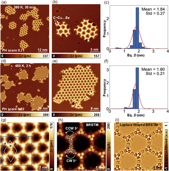
In view of kinetics, further annealing with sufficient time (460 K for 2 h) was applied to the sample, patches of ordered OMs coalesced into larger areas of honeycomb networks as displayed in Figs. 3d and e with an even higher PH score of 0.82, which is very close to a perfectly regular network with PH score of 1. The equivalent diameters of the larger honeycomb networks are characterized by highly narrow distributions with the standard deviation of 0.21 as shown in Fig. 3f, implying a nearly perfect degree of order for the doped network. The average diameter (μ) of the honeycomb network equals to 1.80 nm, which is calculated with the mentioned equation Eq.
From the high-resolution STM image (Fig. 3g), it is clear to identify that the MOF structure features a rhombic unit cell with lattice parameters of a = b = 2.61 ± 0.05 nm and α = 120° ± 2°, in good agreement to the theoretical prediction of a = b = 2.58 nm and α = 120° in gas phase. The bond-resolved STM (BRSTM) images before and after Laplace filtering (Figs. 3h and i) are detected from the region outlined by the blue rectangle in panel (g). The building block in a unit cell contains two monomers and three Cu adatoms. Unexpectedly, one of the monomer moieties rotates by 5° clockwise and the other counterclockwise, rendering the two moieties of the building block chiral but the overall honeycomb network racemic. This is due to the slight molecular flexibility that persists.
STS measurements were carried out on the Cu (111)-supported 2D MOFs at different sites as indicated in Fig. S6 (Supporting information). The reference dI/dV spectrum measured on the Cu (111) substrate shows a Shockley surface state at approximately −450 mV (gray curve in Fig. S6b) [36]. The intrinsic HOMO and LUMO states of the 2D metal organic nanostructure were not observed in the dI/dV spectra (red and black curves recorded on the monomer moiety and Cu adatom, respectively), which could be attributed to the doping effect from Br adsorbates [37,38], as well as the contribution to density of states (DOS) relative to that from the copper substrate [39,40]. To explore the origin of the state, we calculated the DOS for the 2D MOF in gas phase as exhibited in Fig. S6c by DFT. Fig. S6d displays the spin-polarized DOS of the free-standing 2D MOF structure. Intriguingly, the asymmetric DOS for spin-up and spin-down components indicates spin polarized properties, although the incorporated Cu atoms in the chains are not magnetically active, which is similar to our previous studies [41,42]. The corresponding projected DOS (PDOS) on the N, C, H and Cu elements of the 2D MOF was also calculated to show their respective contributions in Fig. S6e.
To investigate the mechanism of Se doping, we performed additional experiments with different ratios of pTBPT to Se (Fig. S7 in Supporting information). All of these samples were thermally treated at 380 K for 2 h following co-deposition of pTBPT and Se. When 0.28 ML pTBPT was deposited onto Cu (111) without Se doping, the disordered OM network composed of polygons with different edges was observed with the PH score of 0.56 as shown in Fig. S7a. Upon deposition of 0.01 ML Se, there still coexisted hexagonal and non-hexagonal polygons in Fig. S7b with the PH score of 0.58. No improvement in the OM networks originates from the insufficient amount of Se compared to the sample in Fig. 3a. Further increasing the coverage of Se to 0.02 ML, an apparent improvement in the proportion of hexagonal OM rings is evident in Fig. S7c with PH score of 0.68, manifesting the structure ordering by Se doping. Some small copper selenide domains were observed adjacent to the ordered hexagonal networks in Fig. S7c. That is to say, the amount of Se is related to the ordering and stabilization of the hexagonal network structure. When the coverage of pTBPT was increased to 0.58 ML, the ordered hexagonal network grows bigger with PH score of 0.70, and fewer copper selenide domains were observed in Fig. S7d. Therefore, we hypothesize that the ordered honeycomb network could be stabilized with the doped Se atoms. The distribution of the equivalent diameters becomes narrow after Se doping by comparison between Figs. S7e-h, illustrating the increased degree of order for the networks following Se incorporation.
Given the low diffusion barrier of Se atoms on Cu (111) (0.107 eV) [43], and the copper selenide domains indicated by white arrows in Fig. S7c do not easily diffuse on Cu (111), we could clearly resolve the trapezoid domains in the STM images. It is plausible that the Se atoms play a pivotal role in regulating the OM networks. Theoretical insights into how Se atoms influence the energy diagrams are provided in the following DFT discussion.
To better understand the mechanism for the disorder−order transition of the 2D OM networks through Se doping, nudged elastic band (NEB) calculations in the absence or presence of Se have been employed to model the transformation between non-hexagonal and hexagonal rings on Cu (111). The molecule is simplified by bromobenzene to reduce the cost of computations. As illustrated in Fig. 4a, the energy barrier was calculated to be 0.76 eV from the five-membered ring accompanied by the sixth radical to the six-membered ring.
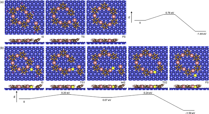
After Se doping, the Se atom locates beside the Cu adatom which is about to leave (intermediate state (IntS), and initial state (IS) in Fig. 4b). During the activation of the organometallic interaction, the adjacent Se atom connects to the C–Cu terminal, which would help to stabilize the intermediate state by C–Cu···Se interaction (IntS in Fig. 4b). The activation barrier from initial state over the first transition state to intermediate state is calculated to be 0.20 eV, followed by the incorporation of the sixth radical with the help of Se. The energy barrier of the second step is calculated to be 0.24 eV. The low transformation barrier of 0.20 eV elucidates the ease with which non-hexagonal OM rings can be transformed to hexagonal OM rings in the presence of Se on Cu (111) surface. The entire pathway is exothermic by 1.59 eV (final state (FS) in Fig. 4b).
The Arrhenius equation is defined as follows (Eq. 1):
|
|
(1) |
where the energy barrier ΔE is defined as the energy difference between the TS and IS, and kB is Boltzmann's constant. The prefactor Apre is normally assigned the rule-of-thumb value of 1013 s−1. To study the influence of the calculated energy barriers on the reaction kinetics, we define the Boltzmann ratio as (Eq. 2):
|
|
(2) |
where ΔE1 equals to 0.20 eV and ΔE2 equals to 0.76 eV in corresponding to the energy barriers in the presence or absence of Se. As a result, the Boltzmann ratio r ≫ 1 in quite a wide range of reaction temperature. Large values of r indicate that the transformation from the non-hexagonal OM ring to the hexagonal OM ring is much easier with the Se atom, which accounts for the disorder−order transition of 2D OM networks after Se doping.
Se doping lowers the transformation energy barrier, thus facilitating the conversion of non-hexagonal OM rings into hexagonal OM rings. On the other hand, higher temperatures would induce demetallation, thereby the ordering of OM networks is resisted. Experimental results indicate that Se doping raises the required temperature for demetallation to above 480 K. Without Se doping, annealing at this temperature typically leads to the coexistence of organometallic and covalent nanostructures. However, with Se doping, such high temperatures enhance the regularity of OM networks rather than triggering demetallation. Hence, the effect of Se doping promotes the ordering of 2D OM honeycomb nanostructures.
Extensive DFT calculations were performed on energy barriers for molecule migration on Cu (111) surface in Fig. S8 (Supporting information). In the migration of the C–Cu moiety, as illustrated in Figs. S8a−c, the moiety has the same orientation in the initial and the final states. Along one principal axis (indicated by red arrows in Fig. S8a) the migration barrier was calculated to be 0.48 eV. While along another principal axis (indicated by black arrows in Fig. S8b), the sliding diffusion was calculated to be 0.29 eV. Migration along the third principal axis is, by symmetry, equivalent to the second direction (black arrows in Fig. S8b). Importantly, in both cases of the more stable initial and final states, the Cu adatoms were located in the more stable fcc sites, while in the transition states, the Cu adatoms were close to the less stable hcp sites. From a chemical point of view, the molecular moiety is physisorbed on the surface (with distances between the triazine cores and the substrate of > 3 Å). Thus, compared with the molecule, the chemisorbed Cu adatoms in the C–Cu moiety play a more important role in the energy diagram. Both fcc and hcp sites are hollow sites, making the configuration more stable than that on top sites, and this explains the low migration energies.
In addition to the migration barriers, the rotation barriers of the C–Cu moiety on Cu (111) were also calculated. The rotation is important for two OM moieties to properly align before combination. Figs. S8d and e illustrate the rotation process where the C–Cu moiety rotates around the fixed triazine core. The moiety in the final state is rotated clockwise by 120° around a normal to the surface going centered at triazine core, compared to the initial state. The rotation is a two-barrier process, where the local minimum constitutes a shallow intermediate state and the global minimum constitutes initial and final states. The energy barrier is calculated to be ≈0.24 eV, indicating how easily the C–Cu moiety change its directions on the Cu (111) surface. Hence, neither the sliding diffusion nor the rotation diffusion processes are rate-limiting steps above RT.
Further annealing of the C–Cu–C OM networks was conducted to investigate the covalent interlinked products. As shown in Fig. S9 (Supporting information), demetallation of the OMs occurred after annealing the sample at 540 K. Regardless of the absence or presence of Se doping, the covalent networks exhibited limited structural order, with PH scores of 0.54 and 0.66, respectively. Incomplete connections typically arise when mobile precursor monomers are blocked from reaching unsaturated reaction sites of the preformed nanostructures. For instance, monomers may be unable to access a randomly formed internal cavity of a 2D nanostructure island due to steric hindrance in 2D confinement, leaving reaction sites in the internal cavity unsaturated. Wrong connections between precursor monomers, here defined as intermolecular C–C bonds, force the monomer into a nonideal position within the structure. They are generally irreversible and can induce further structural defects. The relative conformational flexibility of the monomer backbones allows for connections between deformed monomers when they encounter steric hindrance. This usually leads to heterogeneous structural motifs in the formed nanostructures. The protopolymer of the ordered OM network formed after Se doping does not yield highly ordered covalent nanostructures at elevated temperatures. To optimize this steering strategy, milder activation methods, such as photoactivation, may be more effective than thermal activation.
In conclusion, disordered OM networks comprising polygons with varying edge numbers were obtained after deposition of the conformationally flexible precursor pTBPT on Cu (111) at RT to 420 K. Upon low coverage (~0.015 ML) Se doping of pTBPT, we successfully achieved the ordering in 2D OM networks and enhanced the structural homogeneity, leading to the formation of honeycomb nanostructures. This could be achieved whether pre- or post-exposing the sample to Se, implying that an ordered 2D MOF can be fabricated regardless of the deposition sequence. Furthermore, disorder−order transition could be fulfilled by low coverage (~0.015 ML) Se doping at 360 K, with a higher temperature of 480 K accelerating the process and increasing the proportion of hexagonal OM rings.
Using high-resolution STM/STS including BRSTM at 4 K, we investigated the conformationally flexible precursor pTBPT on Cu (111) substrate and demonstrated the disorder−order transition of 2D OM networks through Se doping. NEB calculations in the absence or presence of Se have been employed to model the transformation from five-membered to six-membered rings on Cu (111) in order to provide mechanistic insights. These findings underscore the pivotal role of Se doping in modulating the energy diagram of the transformation pathway and achieving the desired topology selectivity in the system. The preferential transformation pathway facilitated by the Se atom offers valuable insights into the thermodynamic and kinetic mechanisms governing topology selectivity, enabling the controlled synthesis of tailored metal-organic nanostructures.
The authors declare that they have no known competing financial interests or personal relationships that could have appeared to influence the work reported in this paper.
Liangliang Cai: Writing – review & editing, Writing – original draft, Investigation, Conceptualization. Xinyi Zhang: Writing – review & editing, Investigation. Jiayi Lu: Writing – review & editing, Methodology, Investigation. Juan Xiang: Writing – review & editing, Investigation. Qiang Sun: Writing – review & editing, Methodology, Investigation. Andrew T.S. Wee: Writing – review & editing, Funding acquisition, Conceptualization.
L. Cai and A.T.S. Wee acknowledge financial support from the National Research Foundation Singapore (No. NRF-CRP26-2021RS-0002).
Supplementary material associated with this article can be
found, in the online version, at doi:
W. Guo, C. Li, H. Chen, X. Zhou, K. Wu, Adv. Mater. Interfaces 12 (2024) 2400276.
A. Rabia, F. Tumino, A. Milani, et al., ACS Appl. Nano Mater. 3 (2020) 12178–12187. doi: 10.1021/acsanm.0c02665
M.R. Slot, T.S. Gardenier, P.H. Jacobse, et al., Nat. Phys. 13 (2017) 672–676. doi: 10.1038/nphys4105
W.C. Pan, C. Mützel, S. Haldar, et al., Angew. Chem. Int. Ed. 63 (2024) e202400313. doi: 10.1002/anie.202400313
R. Nemoto, R. Arafune, S. Nakano, et al., ACS Nano 18 (2024) 19663–19671.
X. Li, Z. Xu, D. Bu, et al., Chin. Chem. Lett. 36 (2025) 110100. doi: 10.1016/j.cclet.2024.110100
M. Telychko, G. Li, P. Mutombo, et al., Sci. Adv. 7 (2021) eabf0269. doi: 10.1126/sciadv.abf0269
M. Kunitake, R. Tanoue, R. Higuchi, et al., Nanoscale Adv. 2 (2020) 3202–3208. doi: 10.1039/d0na00180e
X.H. Liu, C.Z. Guan, D. Wang, L.J. Wan, Adv. Mater. 26 (2014) 6912–6920. doi: 10.1002/adma.201305317
D.G. Wang, T. Qiu, W. Guo, et al., Energy Environ. Sci. 14 (2021) 688–728. doi: 10.1039/d0ee02309d
R. Zhang, B. Xia, H. Xu, N. Lin, Angew. Chem. Int. Ed. 58 (2019) 16485–16489. doi: 10.1002/anie.201909278
C. Zhang, E. Kazuma, Y. Kim, Angew. Chem. Int. Ed. 58 (2019) 17736–17744. doi: 10.1002/anie.201909111
G. Galeotti, F. De Marchi, T. Taerum, et al., Chem. Sci. 10 (2019) 5167–5175. doi: 10.1039/c8sc05267k
G. Galeotti, F. De Marchi, E. Hamzehpoor, et al., Nat. Mater. 19 (2020) 874–880. doi: 10.1038/s41563-020-0682-z
D. Wang, X. Lu, Arramel, et al., ACS Nano 16 (2022) 9843–9851. doi: 10.1021/acsnano.2c03909
B. Yang, K. Niu, N. Cao, et al., Angew. Chem. Int. Ed. 62 (2023) e202218211. doi: 10.1002/anie.202218211
M.O. Blunt, J.C. Russell, N.R. Champness, P.H. Beton, Chem. Commun. 46 (2010) 7157–7159. doi: 10.1039/c0cc01810d
R. Gutzler, H. Walch, G. Eder, et al., Chem. Commun. (2009) 4456–4458. doi: 10.1039/b906836h
T. Faury, S. Clair, M. Abel, et al., J. Phys. Chem. C 116 (2012) 4819–4823. doi: 10.1021/jp300417g
O. Ourdjini, R. Pawlak, M. Abel, et al., Phys. Rev. B 84 (2011) 125421. doi: 10.1103/PhysRevB.84.125421
Q. Fan, J.M. Gottfried, J. Zhu, Acc. Chem. Res. 48 (2015) 2484–2494. doi: 10.1021/acs.accounts.5b00168
W. Zhao, L. Dong, C. Huang, Z.M. Win, N. Lin, Chem. Commun. 52 (2016) 13225–13228. doi: 10.1039/C6CC05029H
L. Cai, T. Gao, A.T.S. Wee, Nat. Commun. 15 (2024) 3235. doi: 10.1038/s41467-024-47614-9
Y. Wang, Y. Liu, H. Zou, et al., Appl. Surf. Sci. 609 (2023) 155256. doi: 10.1016/j.apsusc.2022.155256
T. Lu, Q. Chen, Chemistry–Methods 1 (2021) 231–239. doi: 10.1002/cmtd.202100007
T.T.T. Bui, S. Dahaoui, C. Lecomte, G.R. Desiraju, E. Espinosa, Angew. Chem. Int. Ed. 48 (2009) 3838–3841. doi: 10.1002/anie.200805739
D. Peyrot, M.G. Silly, F. Silly, Phys. Chem. Chem. Phys. 20 (2018) 3918–3924. doi: 10.1039/c7cp06488h
J. Tschakert, Q. Zhong, D. Martin-Jimenez, et al., Nat. Commun. 11 (2020) 5630. doi: 10.1038/s41467-020-19379-4
Q. Fan, L. Liu, J. Dai, et al., ACS Nano 12 (2018) 2267–2274. doi: 10.1021/acsnano.7b06787
D. Wang, Z. Wang, W. Liu, et al., Small 18 (2022) 2202368. doi: 10.1002/smll.202202368
L. Cai, Y. Huang, D. Wang, et al., J. Phys. Chem. Lett. 13 (2022) 2180–2186. doi: 10.1021/acs.jpclett.2c00147
A. Gutierrez, M. Buchet, S. Clair, ChemPhysChem 20 (2019) 2286–2291. doi: 10.1002/cphc.201900257
J. Lu, D. Nieckarz, H. Jiang, ACS Nano 17 (2023) 20194–20202. doi: 10.1021/acsnano.3c05945
J. Dai, X. Zhao, Z. Peng, et al., J. Am. Chem. Soc. 145 (2023) 13531–13536. doi: 10.1021/jacs.3c03691
Z. Liang, S. Wu, J. Wang, et al., ACS Nano 17 (2023) 10938–10946. doi: 10.1021/acsnano.3c02819
J. Kliewer, R. Berndt, E.V. Chulkov, et al., Science 288 (2000) 1399–1402. doi: 10.1126/science.288.5470.1399
Z. Yang, T. Sander, J. Gebhardt, et al., ACS Nano 14 (2020) 16887–16896. doi: 10.1021/acsnano.0c05865
Z. Yang, J. Gebhardt, T.A. Schaub, et al., Nanoscale 10 (2018) 3769–3776. doi: 10.1039/c7nr08238j
M. Pan, L. Liang, W. Lin, et al., 2D Mater. 3 (2016) 045002. doi: 10.1088/2053-1583/3/4/045002
D.J. Rizzo, Q. Dai, C. Bronner, et al., Nano Lett. 20 (2020) 963–970. doi: 10.1021/acs.nanolett.9b03998
X. Yu, Q. Sun, M. Liu, et al., Chem. Mater. 34 (2022) 1770–1777. doi: 10.1021/acs.chemmater.1c04015
W. Gao, L. Cai, F. Kang, et al., J. Am. Chem. Soc. 145 (2023) 6203–6209. doi: 10.1021/jacs.2c12292
H. Walen, D.J. Liu, J. Oh, ChemPhysChem 17 (2016) 2137–2145. doi: 10.1002/cphc.201600207

Scheme 1 Structural diagram and reaction pathway. Reaction pathway of pTBPT on Cu (111) toward OMs with different membered rings and ordered hexagonal OMs after selenium doping.

Figure 1 Intact pTBPT on Cu (111) at low temperature. (a) The overview STM image showing isolated monomers and self-assembled domains after deposition of pTBPT on Cu (111) at 90 K. The close-packed directions of Cu (111) are marked by white arrows. (b) The high-resolution STM image of close-packed self-assembled phase, and (c) the corresponding DFT-relaxed model. The unit cells in (b, c) are highlighted in black arrows. Brown, white, gray, and red balls represent C, H, N, and Br atoms, respectively. STM parameters: constant current, (a) U = 1 V, I = 100 pA; (b) U = −1.5 V, I = 50 pA.

Figure 2 Disordered porous OMs on Cu (111) at different preparation parameters. Large-scale (left column) and zoomed-in (middle column) STM images showing disordered porous OMs formed after deposition of pTBPT (a, b) and anneal at 360 K overnight; (d, e) anneal at 380 K for 2 h; (g, h) anneal at 460 K for 2 h; (j, k) on hot Cu (111) substrate held at 440 K. Blue ellipses indicate part of the demetallized C–C interlinks in panels (h) and (k). (c, f, i, l) The distribution of the equivalent diameters. The histograms are fitted by the Gaussian function shown in red, which produce the mean values (Mean) and distributions (Std). pH scores of the corresponding samples are indicated. STM parameters: constant current, (a, b, j, k) U = 200 mV, I = 50 pA; (d, h) U = 1 V, I = 100 pA; (e, g) U = 1 V, I = 50 pA. Panels (e) and (h) are resolved by CO-adsorbed tip.

Figure 3 Crystallization of 2D OM networks on Cu (111) after Se doping. (a) Overview and (b) close-up STM images showing the ordered 2D OM networks fabricated by co-deposition of pTBPT and selenium on Cu (111) after annealing at 380 K for 30 min. (c) The distribution of the equivalent diameters of the sample in panel (a). (d) Overview and (e) close-up STM images showing the ordered 2D OM networks after annealing at 460 K for 2 h. (f) The distribution of the equivalent diameters of the sample in panel (d). The histograms are fitted by the Gaussian function as red curves in panels (c) and (f). (g) High-resolution image of the ordered hexagonal OM. Constant-height current image (h) before and (i) after Laplace filtering of the place framed by the blue rectangle in panel (g). Brown, white, gray, and pink balls represent C, H, N, and Cu adatoms, respectively. PH scores of the corresponding samples are indicated. STM parameters: constant current, (a, b) U = 500 mV, I = 100 pA; (d, e) U = 1 V, I = 50 pA; (g) U = 1 V, I = 100 pA; (h, i) constant height, U = 5 mV. The STM images in panels (d, e, g-i) are resolved by CO-terminated tip.

Figure 4 Disorder−order transformation pathway from 5-membered ring to 6-membered ring in the absence or presence of Se atoms. Energy diagrams for the transformation from 5-membered ring to 6-membered ring (a) without and (b) with Se doping. The structural models are given for the initial, transition, intermediate and final states, respectively. The energy scale is not linear. Brown, white, gray, yellow, blue, and pink balls represent C, H, N, Se, Cu substrate, and Cu adatoms, respectively.

 扫一扫看文章

扫一扫关注我们
 DownLoad:
 下载:
下载:
 下载:
下载: