Citation:
Chang Liu, Jianbo Li, Yijia Wang, Chenguang Liu, Sylvain Pitie, Mahamadou Seydou, Chun Zhao, Paul J. Low, Yannick J. Dappe, Li Yang. Metallocene-based molecule junctions: Electron transport across Au||Au and Au||graphene electrodes[J]. Chinese Chemical Letters,
2026, 37(5): 111811.
doi:
10.1016/j.cclet.2025.111811
Metallocene-based molecule junctions: Electron transport across Au||Au and Au||graphene electrodes
English
Metallocene-based molecule junctions: Electron transport across Au||Au and Au||graphene electrodes
Received Date:
02 April 2025 Accepted Date:
08 September 2025 Revised Date:
06 September 2025 Available Online:
15 May 2026
Abstract:
Metallocenes are a wide family of organometallic compounds, in which two cyclopentadienyl ligands "sandwich" a metal ion, M(η5-C5R5)2, and have considerable potential for use as components in molecular electronics applications. Here we have studied the electronic transport properties of the matallocenes MCp2 (M = V, Cr, Mn, Fe, Co, Ni, Ru; Cp = η5-C5H5) and MCp*2 (M = Mn, Fe, Co; Cp* = η5-C5Me5). Molecular junctions have been fabricated using either two gold, or one gold and one graphene electrode(s), giving rise to single-molecule conductance values of the order of -4 to -3 log(G/G0)) depending on both the nature of the metallocene and the electrode materials. Calculations on model junctions at the density functional theory level of theory reveal significant charge transfer from the metallocene to the junction electrodes and changes in the nature of the primary charge transport pathways in response to the nature of the metal, supporting ligands, molecular oxidation state and electrode composition.
The concepts of an electronic technology based on molecular sub-structures can be traced back to von Hippel's expressions of "molecular engineering" in 1956 [1], and which gave rise to the earliest concepts of the field that we now recognize as molecular electronics [2]. Almost 20 years later, Aviram and Ratner's seminal presentation of a molecular structure designed to serve as a "molecular rectifier" began the process of linking chemical structure to tailored electrical properties [3]. Since then, various molecular structures have been described that serve as mimics of conventional electronic components, including switches [4,5], rectifiers (diodes) [6] and transistors [7]. Electrode|molecule|electrode devices, or "molecular junctions" have proven to be powerful tools with which to explore charge transport mechanisms; for example, by correlating the bias driven current flowing through the molecular junction with chemical structure, phenomena such as incoherent charge hopping, coherent tunnelling and quantum interference effects can be identified and studied. In seeking to expand the range of electrical responses offered by molecular junctions, attention has been increasingly drawn to metal complexes as functional backbones and head groups [8].
The majorities of metal complexes incorporated within molecular junctions have the common anchor-backbone-anchor structure, with the metal fragment within the backbone serving to tune frontier orbital energies and modulate conjugation [9–11], and introduce electrical response within the junction beyond wire-like charge transfer, such as rectifying characteristics [12–15]. The sensitivity of metal d-orbital splitting to the local geometry, the basis of which is broadly captured within the concepts of ligand-field theory, leads to further opportunities for control of metal-complex based molecular junctions through mechanical manipulation [16,17]. The partial occupancy of the d- (and f-) orbitals also engenders opportunities for introduction of spintronic behaviour [18–21], and enhance thermoelectric effects [22], whilst the facile redox properties associated with many metal compounds and complexes leads to potential for switching [23,24] and electrochemical gating within the junction [25].
Against this background of the emerging role of metal complexes in molecular electronics, the potential for metallocenes to be used for the construction of MJs has been recognized [26–28]. Metallocenes are a general family of complexes composed of a single metal atom (or ion) sandwiched between two cyclopentadienyl (η5-C5H5, Cp) rings, and substituted derivatives. By varying the metal atom and/or the peripheral substitution of the Cp ligands, the redox properties of the isolated complexes and frontier orbital energies can be fine-tuned, making them appealing components for use in molecular electronics [29]. In addition, both eclipsed (D5h) and staggered (D5d) conformations exist, with a relatively small rotation barrier of approximately 0.05 eV in the case of the iron(Ⅱ) metallocene, ferrocene [30]. This facile rotation allows the metallocene to adopt a series of different geometries within the junction as the junction evolves in response to modulation of the electrode separation, which strongly influence the junction conductance [31–34]. However, as a result of this facile rotation, metallocenes featuring 1,1′-substitution of the Cp rings with anchor groups can adopt 'hairpin' structures, with both anchors contacting to the same electrode surface [35,36]. Nevertheless, ferrocene has emerged as a highly promising candidate for the development of dynamic molecular switches and associated circuit components, owing to its distinctive electronic and electrochemical properties, configurational tunability, and well-established research foundation across diverse applications [37].
Whilst molecular design strategies that allow the statistically favoured assembly of 1,1′-functionalised metallocene molecular junctions remain a topic of interest [22,38–43], a growing body of work has been directed to molecular junctions formed with the parent metallocenes, MCp2 [44]. In these simple electrode|MCp2|electrode junctions it has been proposed that the electrodes make contact with either both Cp ring-systems [28,45] or through one Cp ligand and the metal ion [46,47]. When contacted to the electrodes through the π-face of the "top" and "bottom" Cp ligands, the electrical behaviour of these metallocene junctions is also sensitive to mechanical compression [48], and near to resonant transport is observed when sufficiently strong molecule-electrode coupling is achieved.
We were drawn to consider metallocene junctions featuring metals with different formal valence electron counts formed on a nickel-supported graphene electrode, with a gold STM tip serving as top contact. The experiments were conducted under ambient conditions and the tip bias was set to 0.3 V for STM-I(s) measurements. The amount of data collected in the experiments is provided in Tables S3 and S4 (Supporting information). To explore the effects of the asymmetric electrode environment on the electrical characteristics, reference data were also collected using a gold-on-glass substrate via the STM-I(s) method [49] to avoid complications that might arise from competing contacts to the metal ions observed under STM-break junction conditions [36,47].
The electronic configuration of the d-orbital electrons, the energy level positions, and the ligand field effects of the metal center directly influence the electronic transport properties of the molecule. By comparing isostructural complexes featuring different metal centers in their chemical composition, the influence of metal atoms on the molecular orbital energy levels and charge distribution can be clearly elucidated. Moreover, the interaction between the metallocene and the electrode surface is a key factor in determining single-molecule conductance. Different metal centers may modulate the charge tunnelling efficiency by altering the surface electrostatics and interfacial barriers between the molecule and the electrode.
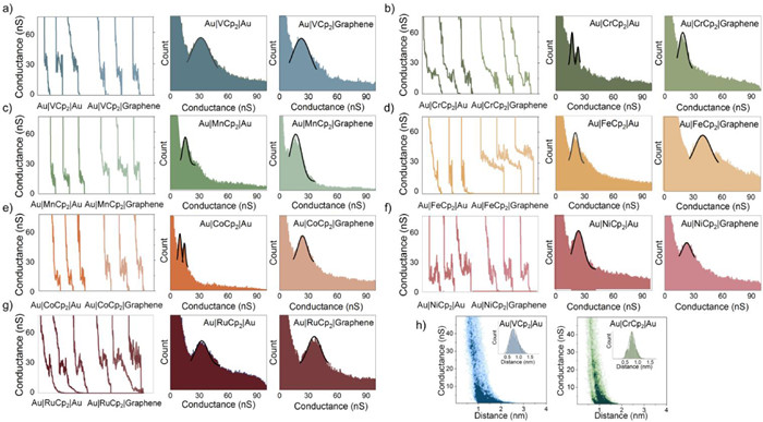
Individual conductance traces measured by STM-I(s) method and the corresponding 1D histograms obtained through the statistical analysis of these data for symmetric gold-gold and asymmetric gold-graphene molecular junctions are displayed in Fig. 1. The plateau regions in the distance-current curves correspond to events where molecules are connected between the two electrodes. The plateau regions of the I(s) traces feature pronounced "jump" or sloped features, which indicate the transition of the metallocenes between different junction geometries and binding sites as the electrode separation is increased [50]. For the binning parameters employed here, the plateau features arising from these junction configurations lead to an apparent double peak in the conductance histograms plotted from the gold-gold junctions formed with CrCp2 and CoCp2, the average of which is taken as an approximation of the 'most probable' molecular conductance. Each selected conductance-distance profile is subjected to frequency histogram analysis, resulting in a two-dimensional conductance-distance statistical map. In this representation, each point corresponds to a one-dimensional conductance-distance curve, with the density of points indicated by colour intensity. Deeper colour shades signify a higher concentration of conductance values at specific distance positions. The two-dimensional statistical map provides a comprehensive visualization of the molecular junction conductance distribution. As illustrated in Fig. S1 (Supporting information), the conductance distribution pattern in the 2D map aligns with that observed in the 1D profiles. Additionally, the distance histogram reveals the distribution of molecular junction stretching lengths, offering further insights into the system's characteristics. In the corresponding 2D histograms of conductance counts for Au|CrCp2|Au and Au|CoCp2|Au two regions of high data density provide further indications of the presence of multiple junction configurations.
Figure 1
Figure 1.
STM-I(s) conductance traces and 1D conductance histograms of (a) VCp2, (b) CrCp2, (c) MnCp2, (d) FeCp2, (e) CoCp2, (f) NiCp2, and (g) RuCp2 in Au||Au electrode and Au||graphene electrode molecular junctions. (h) 2D histograms of the conductance of Au|VCp2|Au and Au|CrCp2|Au molecular junctions.
The conductance values from across the series of metallocenes MCp2 examined here fall in a relatively narrow range in both gold-gold (CoCp2: G = 9.8 nS; log(G/G0) = −3.90. VCp2: G = 32.5 nS; log(G/G0) = −3.38) and gold-graphene (MnCp2: G = 16.8 nS; log(G/G0) = −3.66. FeCp2: G = 39.8 nS; log(G/G0) = −3.29) junctions. Nevertheless, sufficient differences are apparent over the ca. 2–3 fold conductance range to determine that the molecular conductance values are sensitive to both the nature of the metal ion within the metallocene, and the electrode material combination (Table 1). In the broadest of terms, such variation can be attributed to changes in the alignment of molecular frontier orbital energies with the electrode Fermi levels, which convolutes the redox state of the molecule within the junction, the molecule-electrode coupling and most stable junction geometry [51]. Although charge transfer magnitudes are comparable in Au|ferrocene|Au and Au|ferrocene|graphene junctions, the distinct electrode properties induce markedly different electrostatic environments. Consequently, in Au|ferrocene|Au junctions, the Fermi level resides within the molecular gap, aligned closer to the LUMO. In stark contrast, for Au|ferrocene|graphene, the Fermi level approaches the HOMO. This near-pinning of the HOMO to the Fermi level significantly enhances conductance, accounting for the order-of-magnitude difference observed between the two systems. The origin of this electrostatic contrast lies in junction-dependent interfacial dipoles, consistent with our prior work [52].
Table 1
Table 1.
The conductance values and calculated zero-bias charge transfer from the (decamethyl)metallocene to the electrodes in Au||Au (left) and Au||graphene (right) junction.
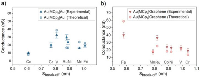
When comparing 1D histograms for Au||Au and Au||graphene junctions (Fig. 1), the peak widths for Au||graphene junctions are generally wider than those of the corresponding gold-gold junction, likely indicating a greater range of junction geometries and hence molecule-electrode couplings at the graphene electrode. The break-off distances determined by the STM-I(s) method are free of the additional complications of the electrode snap-back [53], and fall in a fairly narrow range for both the Au||Au (0.61–1.01 nm) and Au||graphene (0.58–1.04 nm) junctions (Figs. S1 and S2 in Supporting information). Whilst these values are broadly consistent with the geometry of "parallel" molecular junctions with the electrodes contacting to the Cp rings, noting the Cpcentroid···Cpcentroid distances in the metallocenes (0.33–0.41 nm) and the Au···Cp (ca. 0.2 nm) or graphene···Cp (ca. 0.3 nm) contacts, there is no direct correlation of the statistically averaged break-off distances to the dimensions of the specific molecule in each junction, reflecting the weak van der Waals contacts, the diverse junction geometries and the variation in electrostatic contributions in each case. However, with the exception of the anomalously low conductance of the Au|CoCp2|Au junction, the junction conductance generally decreases with increasing junction length (Fig. 2).
Figure 2
Figure 2.
Conductance trends with break off distance between Au||Au electrodes (a) and Au||graphene electrodes (b).
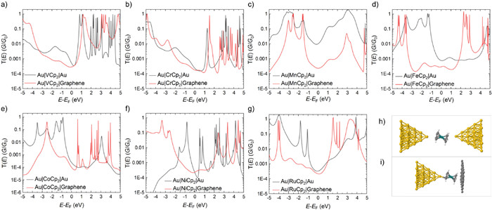
To better explore the complex structure-property relationships in these deceptively simple molecular junctions, model systems were constructed from 35-atom gold pyramidal electrodes [38] and 5 × 5 monolayer graphene sheets. The junction structures were optimized until the forces went below 0.05 eV/Å. From these optimized molecular junctions, the electronic transport was determined using a non-equilibrium Green's function (NEGF) formalism included in Fireball, within the Fisher-Lee approach [54,55]. As a general remark, the configurations leading to transmission curves that best model the experimental data (Fig. 3) involve a weak coupling between the metallocene and the gold electrodes. As an exception, in the vanadium case, there is a more pronounced interaction with the electrodes leading to a significant distortion of the metallocene structure towards a C2v geometry (Fig. S3a in Supporting information), and accounting for the relatively high single molecule conductance of this species (Table 1). Model molecular junctions formed with smaller electrode gaps and closer electrode-molecule contacts gave transmission (and hence conductance) values one or two orders of magnitude greater than the experimental values obtained from the STM-I(s) experiments performed here, but closer to the very high (0.1–0.25 G0) values obtained from break-junction measurements [44,56]. These data are consistent with observations of mechanically gated molecular conductance in ferrocene-based junctions contacted to silver electrodes through the Cp ligands [48].
Figure 3
Figure 3.
Calculated electronic transmissions for the different metallocene junctions for (a) vanadocene, (b) chromocene, (c) manganocene, (d) ferrocene, (e) cobaltocene, (f) nickelocene, and (g) ruthenocene. DFT-optimized configurations for ruthenocene molecular junctions between (h) Au||Au and (i) Au||graphene electrodes.
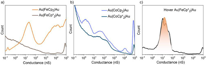
A strong electrostatic dipole at the metallocene|gold interface results in a charge transfer from the molecule to the electrode (Table 1) [38]. The weaker van der Waals contacts to the graphene electrode typically leads to a reduced charge transfer from the molecule, and broader plateaus in the transmission function near E - EF = 0 eV. Plots of the calculated junction orbitals that dominate electronic transport are shown in Fig. S6 (Supporting information). For the earliest metal examples (VCp2, CrCp2), the Cp ligands contribute strongly to the overall electronic structure of the junctions near the Fermi energy, with the metal d-orbitals featuring more significantly in the cases of MCp2 (M = Mn, Fe, Ru, Ni). However, in the case of the Au|CoCp2|Au junction the LUMO features little molecular character. Assuming a predominantly electron (as opposed to hole) transfer based charge transfer mechanism in these junctions, this may account for the low conductance observed in this case. This is reflected in the transmission function T(E) near the Fermi level, which is ca. 2–3 times lower than the configurations with other metals (Fig. 3). Compared with previous studies on ferrocene-containing molecular junctions using break-junction approaches [45,57], the lower conductance observed in these measurements likely arises from the greater minimum electrode spacing maintained in the STM-I(s) methodology, which enforces fully extended conformations of ferrocene molecular units and limits electrode-Fe contacts, and blunter tips which contact the π-face of the "top-contact" Cp ligand. This elongated configuration increases interfacial strain and reduces electron tunnelling efficiency relative to relaxed molecular geometries in dynamic junction techniques. Despite the presence of the peripheral methyl groups, the decamethylmetallocenes MnCp*2, FeCp*2 and CoCp*2 all form both gold-gold and gold-graphene junctions via the STM-I(s) method (Fig. S9 in Supporting information). As might be expected, these more electron-rich permethylated systems give rise to even greater charge transfer to the gold electrodes than the Cp analogues, and as with the Cp examples the molecular conductance in the asymmetric gold-graphene junctions is similar or somewhat greater than the gold-gold examples (Table 1), likely a consequence of the graphene-Cp* -stacked contacts (Fig. S10e in Supporting information). An STM-BJ experiment with FeCp2 and gold electrodes revealed two conductance features over a large conductance window (log(G/G0) = 1.0–10–6) (Fig. 4). The higher conductance feature gave rise to a broad envelope in the 1D conductance histogram, with a most probable molecular conductance of log(G/G0) = −0.81 (11, 988 nS), which corresponds to the feature observed by Aragonès in a much narrower conductance window (log(G/G0) = 1–10–2) [45]. The lower conductance peak (log(G/G0) = −3.59; 19.6 nS) is consistent with the junction formed by the I(s) method (Table 1, Fig. 1). To expand the data set, STM-BJ measurements of CoCp2 were also made, revealing a series of high (H: log(G/G0) = −0.8; 12, 280 nS), medium (M: log(G/G0) = −3.50; 24.3 nS) and low (L: log(G/G0) = −4.65; 1.7 nS) conductance features (Fig. 4). Clearly, the initial pre-assembly of the metallocene on the thinning gold filament extruded between the STM tip and substrate can give rise to a junction in which the metallocene is more strongly coupled upon rupture of the last metal-metal bond to give atomically sharp tips [58,59]. Whilst this arguably supports the critical role of electrode shape in the electrical properties of the junction [28], conductance features arising from Cp-contacted junctions are almost invariably lower than these high conductance features. Rather it appears that the initial junctions formed in the break junctions likely involve at least one Au···Fe (or Co) contact [46]. In further support on this concept, it is noted that efforts to form and measure the high conductance single-molecule junctions from the peripherally substituted FeCp*2 (Fig. 4a) and CoCp*2 (Fig. 4b) complexes, with the methyl groups shielding access for the electrode(s) to the sandwiched metal atom, by the STM-BJ method failed. Subsequently, the STM-BJ tip retraction routine was modified such that when the system detected a conductance signal –5 < log(G/G0) < –3 during the retraction step, the motion of the tip was paused for 100 ms, allowing for equilibration of the junction formation processes. In this "hover" experiment, a clear peak in the 1D conductance histogram is formed from FeCp*2 near log(G/G0) = –3.68 (16.2 nS), which matches the feature observed in the I(s) data, and the same order of magnitude as the lower conductance feature from STM-BJ experiments. These observations are consistent with a model in which the atomically sharp tips formed on cleavage of the metallic filament in the early stages of the STM-BJ and at closest electrode separations form junctions in which the MCp2 metallocenes are contacted through a Cp ligand and the more accessible metal ion, giving rise to a high conductance state, which evolves on further separation of the electrodes to the lower conductance "parallel" junctions in which the electrodes contact the metallocene through the -faces of the "top" and "bottom" Cp-ligands in a manner favoured by the STM-I(s) junctions formed with blunter electrode tips. The steric crowding of the sandwiched metal ion by the Cp* ligands prevents the initial high conductance contact in the STM-BJ experiment. During junction stretching, multiple conductance features are observed, reflecting dynamic evolution of the junction geometry [60].
Figure 4
Figure 4.
1D conductance histograms of: (a) FeCp2 (in orange) and FeCp*2 (in brown), (b) CoCp2 (in blue) and CoCp*2 (in indigo) collected from STM-BJ experiments with Au||Au electrodes. (c) 1D conductance of Au|FeCp*2|Au generated from modified STM-BJ measurements when the gold tip was allowed to hover for 100 ms after detection of conductance signals log (G/G0) = –3 to –5.
In the present work, we have studied both experimentally and theoretically the electronic transport properties of metallocene-based molecular junctions. Using either two gold electrodes or one gold and one graphene electrodes, we have measured the electronic conductance of metallocenes through STM-I(s) experiments. For a range of metallocenes, the most probable molecular conductance lies around 10–40 nS. The introduction of a graphene electrode breaks the symmetry and modifies the transmission levels, but only subtly affecting the conductance value. These STM-I(s) junctions are likely formed from contact between the electrodes and the planar-faces of the Cp ligands whereby significant charge transfer from the metallocene to the gold electrode(s) leads to an electrostatic stabilization of the junction. These -contacted metallocene junctions are several orders of magnitude less conductive than the initial junctions formed by the STM-BJ method with gold electrodes, which likely involve electrode contacts to the sandwiched metal ion. This work brings further insight into the formation, evolution and electrical characteristics of metallocene-based molecular junctions and associated electronic transport properties, highlight potential for further study and use in future molecular devices.
Declaration of competing interest
The authors declare that they have no known competing financial interests or personal relationships that could have appeared to influence the work reported in this paper.
CRediT authorship contribution statement
Chang Liu: Writing – original draft, Methodology, Investigation, Formal analysis, Data curation, Conceptualization. Jianbo Li: Writing – original draft, Methodology, Formal analysis. Yijia Wang: Writing – review & editing, Investigation, Formal analysis. Chenguang Liu: Writing – review & editing, Investigation, Data curation. Sylvain Pitie: Software, Methodology, Investigation, Formal analysis, Conceptualization. Mahamadou Seydou: Software, Formal analysis, Data curation. Chun Zhao: Writing – review & editing, Validation, Supervision, Formal analysis. Paul J. Low: Writing – review & editing, Supervision, Investigation, Formal analysis, Data curation. Yannick J. Dappe: Writing – review & editing, Visualization, Resources, Methodology, Investigation, Data curation, Conceptualization. Li Yang: Writing – review & editing, Supervision, Resources, Project administration, Investigation.
Acknowledgments
The authors thank the support received from the Suzhou Science and Technology Development Planning Program (No. SYC2022101), the Suzhou Industrial Park High Quality Innovation Platform of Functional Molecular Materials and Devices (No. YZCXPT2023105), the XJTLU Advanced Materials Research Center (AMRC), Industrial Cooperative Fund (No. RDS10120220070) from the BAOSHENG (Suzhou) Energy Technologies Co., Ltd., and the XJTLU Research Development Fund (No. RDF-21-01-040). P. J. Low gratefully acknowledges support from the Australian Research Council (No. DP220100790).
Supplementary materials
Supplementary material associated with this article can be found, in the online version, at doi:10.1016/j.cclet.2025.111811.
M. Naher, D.C. Milan, O.A. Al Owaedi, et al., J. Am. Chem. Soc. 143 (2021) 3817–3829. doi: 10.1021/jacs.0c11605
[52]
Q. Zhang, C. Liu, S. Tao, et al., Nano Lett. 16 (2017) 6534–6540.
[53]
W. Hong, D.Z. Manrique, P.M. García, et al., J. Am. Chem. Soc. 134 (2012) 2292–2304. doi: 10.1021/ja209844r
[54]
D.S. Fisher, P.A. Lee, Phys. Rev. B 23 (1981) 6851–6854.
[55]
S. Pitié, M. Seydou, Y.J. Dappe, et al., Chem. Phys. Lett. 787 (2022) 139273.
[56]
Q. Zhou, K. Song, G. Zhang, et al., Nat. Commun. 13 (2022) 1803.
[57]
Y. Li, N. Haworth, L. Xiang, et al., J. Am. Chem. Soc. 139 (2017) 14699–14706. doi: 10.1021/jacs.7b08239
[58]
T. Fu, K. Frommer, C. Nuckolls, L. Venkataraman, J. Phys. Chem. Lett. 12 (2021) 10802–10807. doi: 10.1021/acs.jpclett.1c03160
[59]
S. Yuan, Y. Chen, X. Wang, et al., Chin. Chem. Lett. 36 (2025) 110816.
[60]
W. Xu, H. Zhang, Y. Zhou, et al., J. Am. Chem. Soc. 147 (2025) 5879–5886. doi: 10.1021/jacs.4c14656
Figure 1
STM-I(s) conductance traces and 1D conductance histograms of (a) VCp2, (b) CrCp2, (c) MnCp2, (d) FeCp2, (e) CoCp2, (f) NiCp2, and (g) RuCp2 in Au||Au electrode and Au||graphene electrode molecular junctions. (h) 2D histograms of the conductance of Au|VCp2|Au and Au|CrCp2|Au molecular junctions.
Figure 3
Calculated electronic transmissions for the different metallocene junctions for (a) vanadocene, (b) chromocene, (c) manganocene, (d) ferrocene, (e) cobaltocene, (f) nickelocene, and (g) ruthenocene. DFT-optimized configurations for ruthenocene molecular junctions between (h) Au||Au and (i) Au||graphene electrodes.
Figure 4
1D conductance histograms of: (a) FeCp2 (in orange) and FeCp*2 (in brown), (b) CoCp2 (in blue) and CoCp*2 (in indigo) collected from STM-BJ experiments with Au||Au electrodes. (c) 1D conductance of Au|FeCp*2|Au generated from modified STM-BJ measurements when the gold tip was allowed to hover for 100 ms after detection of conductance signals log (G/G0) = –3 to –5.
Table 1.
The conductance values and calculated zero-bias charge transfer from the (decamethyl)metallocene to the electrodes in Au||Au (left) and Au||graphene (right) junction.

 DownLoad:

 下载:
下载:


 下载:
下载:
