Citation:
Xiaoqing Wu, Yajie Chen, Dagui Wang, Song Pu, Qiujiao Du, Pengcheng Gao. Balancing switching and transient response for ion gating in field-effect nanofluidic transistors[J]. Chinese Chemical Letters,
2026, 37(1): 111623.
doi:
10.1016/j.cclet.2025.111623
Balancing switching and transient response for ion gating in field-effect nanofluidic transistors
English
Balancing switching and transient response for ion gating in field-effect nanofluidic transistors
Received Date:
14 April 2025 Accepted Date:
22 July 2025 Revised Date:
16 July 2025 Available Online:
15 January 2026
Abstract:
Field-effect nanofluidic transistors (FENTs), biomimicking the structure and functionality of neuron, act as biological transistors with the ability to gate switching responses to external stimuli. The switching ratio has been verified to evaluate the performance of FENTs, but until recently, the response time, another crucial indicator, has been ignored. Employing finite-element method, we investigated the relationship among gate charge, switching ratio and response time by divisionally manipulating gate charge, including entrance surface and the surface of confinement space, for ion transport to optimize switching capability. The dual-split gate charge on FENTs exhibits synergistic effect on switching response. Based on the two regional gate charge on FENTs, multivalence ions in lower concentration, high aspect ratio and single channel show higher switching ratio but longer response time compared to monovalent ions. The findings highlight the necessity of balancing these two signals in FENTs and offer insights for optimizing their design and expanding applications to dual-signal-detection iontronics.
Neuron with nanoscale selectivity filters of biological ion channels enables to switch responses to external stimuli, allowing ultra-fast and precise transport of target ions so as to maintain important biological activities in sensory nervous system, including perception, processing, and decision-making [1–4]. Over the past few decades, great efforts have been made to develop a series of bionic biological ion channels by mimicking the structure and operation of neuron for successfully application in life science [5], memory [6,7] and sensing [8–13]. Currently, traditional transistors for computation and signal propagation principally rely on electrons as carriers, offering fast response and high signal amplification [14–17]. However, the high working voltage and the poor biocompatibility have hindered their widespread implementation, particularly in burgeoning areas like artificial neural network and brain-computer interface. Inspired by biological ion channels, the concept to ion transistors that employ ions as carriers have emerged [18–22]. Nonetheless, ions with lower mobility compared with electrons in traditional transistors carry more chemical information to permit selective regulation of various functions and processes within transistors [23,24]. Besides, since ions also serve as carriers in biological transistors, ion transistors possess compatibility with biological signals, promising for applications in artificial intelligence [25–28].
Field-effect nanofluidic transistors (FENTs) have drawn great attention in ion transistors, due to their large capacitance, strong carrier induction capability and low working voltage [18,29,30]. These are similarly to traditional transistors, with the gate voltage or charge controlling the channel current. Generally, FENTs take advantage of geometric confinement effect and charge effect to manipulate electric double layer (EDL) by adjusting geometry [31,32], surface charge [33–37] and probe molecules modification [38–41], which provides opportunities for applications in sensing detection covering ions [10,42], small molecules [43], nucleic acid molecules [44–47] and proteins [48], even in the memory devices [6,49] such as memristor. The properties of FENTs modulated by surface charges have been verified understanding thus far, with accumulating experimental evidence for regulating along the narrow channel configuration [50,51]. This approach of controlling the surface charge of the channel on the gate obtains a benefit to enhance the switching ratio [52–54]. Until now, switching ratio has been employed as gold standard to evaluate the performance of FENTs. However, the relationship between response time, another crucial but neglected indicator, and gate charge is still not explicit in FENTs.
Herein, we report that the divisional regulation of surface charge on entrance surface and the surface of confinement space in FENTs to study the role of gate charge, switching ratio and response time (τ), as well as the interplay between these performances. To this end, transport simulations have been executed using a theoretical approach by numerical simulations, which combines steady-state model for the calculations of switching ratio with transient model for the calculations of τ. To distinguish the key factor of divisional surface charge, we investigated different mechanisms including salt concentration, aspect ratio, channel density and ions with the valence of ±1, ±2, ±3 in FENTs. Our results clearly indicate that trivalent ions in low concentration, high aspect ratio and single channel, exhibit higher switching ratio but longer τ. Compared with trivalent ions, monovalent ions have a relatively lower switching ratio, approximately one orders of magnitude less than trivalent ions, along with a shorter τ. Therefore, it is necessary to make a trade-off in these two signals for nanofluidic transistors. These findings help to optimize the design of FENTs and extend to the manufacture of dual-signal-detection iontronics.
Typically, the simulations of nanofluidics employ numerical calculations especially, finite-element method, which offers a simplified model and short computation time [55,56]. Thus, we performed these calculations using the commercial multiphysical field software COMSOL to investigate the role of divisional regulation of surface charge on ion transport. The geometry in our simulations is shown in Fig. 1a. Details on the parameters and boundary conditions are provided in Supporting information. To explore the responsiveness of FENTs by gate charge controlling, we utilized in the potential range of −1.0 ~ +1.0 V under the transmembrane voltage (Vt) to calculate the ionic current (It) through the FENTs using steady-state solver. Note that surface charge is utilized to serve as gate voltage as E external electric fields in this article [57,58]. The relationship between the “ON–OFF” state of It and bias voltage is schematically shown in Fig. 2a. Because of the channel with negative gate charge, it creates a charge-attraction interaction that facilitate cations entry in the channel at positive Vt, indicating the “ON” state (Fig. 1b, left). While cations only move with the Vt without gate charge controlling, indicating the “OFF” state (Fig. 1b, right).
Figure 1
Figure 1.
Simulative setup and “ON–OFF” state of ionic current. (a) Schematic of simulation model. The surface of the FENTs with length L and channel diameter D, was separation into three regions: entrance surface, the surface of confinement space and exit surface. The gate charge can be manipulated by regulating the surface charge of these regions. (b) Schematics of “ON” and “OFF” states of ionic current.
Figure 2.
Divisionally manipulated gate charge to control ion transport. (a) Schematic of relationship between the “ON–OFF” state of It and gate charge. (b) The contour map of ION/IOFF regulated by entrance-surface charge (σE) and the charge of confinement space surface (σC) with 0.1 mmol/L KCl solution. ION: high-current end at transmembrane bias +1 V for gate with charge; IOFF: low-current end at transmembrane bias +1 V for gate without charge; the switching ratio is calculated as ION/IOFF, and the result is taken as a positive value. The solid black dot represents the FENTs without gate charge. (c) The contour map of ionic conduction regulated by σE and σC with 0.1 mmol/L KCl solution. The white dashed line represents the value of valley bottom, and the solid black dot represents minimum value (equal to 1).
With this configuration, in order to imitate the voltage applied on the gate, surface charge density (σ) ranging from −5 mC/m2 to 5 mC/m2 are selected to apply to the entrance surface and the wall of confinement space, respectively. According to the Gauss’s law, the gate voltage (Vg) can be calculated as Vg = σD/(2ε0) form surface charges, where Vg is ranging from −5.6 V to 5.6 V. ε0 is the permittivity of vacuum. These parameter settings are comparable to that of other nanofluidic transistors [57,58]. The phenomenon of high switch ratio (defined as ION/IOFF in this article) is observed at high σE and low σC, as shown in the green area of Fig. 2b. It indicated that entrance surface charge and the charge of confinement space exhibit synergistic effect on regulating ION/IOFF. Subsequently, the contour map of rectification ratio is seen in the Fig. S2 (Supporting information), which clearly demonstrates the field-effect tunability over ionic diode property with devices of a dual-split gate charge. Considering that the mobility of carriers is also a criterion for evaluating the performance of the FENTs, the ionic conductance (G) can be determined to measure, calculated as G = ION/V. The contour map exhibits that G increases with the surface charge including σE and σC (Fig. 2c). We attribute the result to synergistic effect on the surface of confinement space in alliance with entrance surface to facilitate the passage of ions in the channel. Moreover, the distribution maps and the profiles along Z-axis of net ions concentration illustrate the distribution of ions within the channel, which further confirms the enhancement of ionic conductance (Figs. S3 and S4 in Supporting informaton).
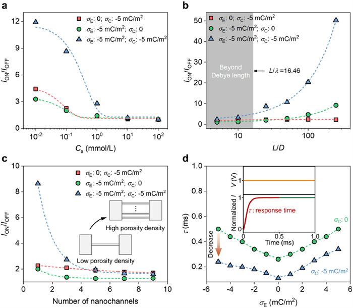
To gain more insight into the effect of entrance surface charge and charge of confinement space on ionic current switching state, we investigated switching capability under different salt concentration (Cs), aspect ratio (L/D) and channel density, respectively. Subsequently, three features of surface charges were selected: (1) σE = 0, σC = −5 mC/m2; (2) σE = −5 mC/m2, σC = 0; (3) σE = −5 mC/m2, σC = −5 mC/m2. When both the entrance surface and the confinement space of the channel are charged, the channel exhibits the maximum ION/IOFF. In contrast, if only one of them carries surface charges, the ION/IOFF of channel decreases significantly. It indicated that synergistic effects of entrance surface charge and the charge of confinement space surface on enhancing the ION/IOFF. As for the effect of salt concentration, the decrease of ION/IOFF with Cs and with entrance surface charge is observed beyond a threshold concentration (10 mmol/L). The lower the salt concentration, the higher ION/IOFF (Fig. 3a and Fig. S5 in Supporting information). In view of the aspect ratio, ION/IOFF increases with L/D, while as L/D crosses from less than L/λ to more than L/λ, ION/IOFF rises rapidly (Fig. 3b). These results demonstrate a strong correlation between the switching capability of the FENTs and the position and size of the EDL. Regarding channel density, the ION/IOFF decreases as the channel density increases, while the G increases in agreement with experimental findings reported in the literature (Fig. 3c and Fig. S6 in Supporting information) [59]. These results suggest that there is an increase in the thickness of FENTs with enhanced ionic conductance, while the switching ratio of FENTs decreases. Overall, it is necessary to manufacture a FENTs with overlapping EDL apertures and single channel in order to achieve a high switching ratio.
Figure 3
Figure 3.
The effect of dual-split gate charge on switching capability. Switching ratio (ION/IOFF) as a function of different Cs (a), L/D (b) and channel density (c). λ is the Debye length, which can be calculated as shown in Section S4 (Supporting information). The values of red symbols are equal to 1. (d) τ as a function of entrance surface charge (σE). The insets: potential control scheme (top) and “ON” state response (bottom) of ionic current (I) with constant bias voltage at +1 V and 0.1 mmol/L KCl solution. Normalized I is corresponding time-dependent normalized current response. The red line delimits the range in which reaching equilibrium state can be used to extrapolate τ. Dashed lines are guide for eyes.
The time scale for ion accumulation and establishment in the channel is defined as the response time (τ). τ of this model controlled by the dual-split gate charge using transient solver, has been investigated. The ionic current was monitored by applying constant bias voltage (+1 V) to measure response time with 0.1 mmol/L KCl solution (Fig. 3d, inset). It is seen that the τ increases with an increase in entrance surface charge when the gate charge is positive; it decreases as charge increases when the gate charge is negative (Fig. 3d). Interestingly, dual-split gate charge contributes to reducing the τ by approximately half significantly, owing to the charged surface of confinement space facilitating the ion transport. Furthermore, the presence of dual-split gate charge raises switching ratio, shown in Fig. 1b Hence, dual-split gate charge on the entrance surface and the surface of confinement space promotes the enhancement of switching capability of FENTs. On the contrary, the presence of gate charge on the confinement space’ wall diminishes the asymmetry of channel, resulting in a decrease in the rectification ratio, which it is the different between nanofluidic transistor and ionic diode devices (Fig. S7 in Supporting information).
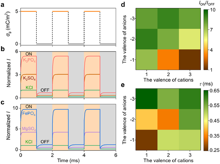
We further probed how ions with different valence influences switching capability of FENTs. Note that the same ionic strength of solutions was selected in the FENTs (KCl, 0.1 mmol/L; MgCl2 and K2SO4, 0.067 mmol/L; FeCl3 and K3PO4, 0.05 mmol/L), in order to allow the ions to transport in EDL. Furthermore, the impact of ionic hydration sizes on ionic current can be neglected in our system, as the nanochannel size of 20 nm surpasses the ionic hydration size. By repeatedly switching the dual-split gate charge (σg) from 0 to +5 mC/m2, the “ON–OFF” state of the ions were detected (Fig. 4a). It is seen that ion transport happens rapidly with time at +5 mC/m2. When σg is switched to 0, the transport immediately stops (Fig. 4b). Furthermore, the behavior of multivalent cations transport is similar with that observed in multivalent anions (Fig. 4c). As expected, high-valence ions exhibit large transmembrane ionic current, due to strong electrostatic interaction between ions and channel wall with decreasing energy barrier. This sequence with “ON–OFF” switching capability can be repeated over several cycles.
Figure 4
Figure 4.
Switching properties of FENTs based on different carriers. Gate charge control scheme (a), the “ON–OFF” response of anionic carriers in FENTs under Vt at +1 V (b) and cationic carriers in FENTs (c). The heat map of ION/IOFF (d) and τ (e) with the valence of ions ranging from −3 to +3.
To evaluate the switching capability, we measured switching ratio and response time. Figs. 4d and e show the ION/IOFF and τ in a valence of ions range from −3 to +3 (Fig. S8 in Supporting information). The anions with the valence of −3 have the higher ION/IOFF (in the top of the heat map) than lower valence anions, which indicates that the switching ratio is strongly related to the gate charge. On the contrary, the anions with the valence of −3 have the lower τ (in the top of the heat map) than lower valence anions. Furthermore, anions have a greater effect on response time than cations (green areas in the upper part and yellow areas in the lower part). The τ of ions can be attributed to different mobilities of ions. Higher ion mobility leads to faster ion movement rates within the channel, reducing the time required for ion accumulation and consequently resulting in a shorter τ. At the meanwhile, we measured the rectification ratio and the response time of the ionic diodes, almost the same conclusion as that of the nanofluidic transistors (Fig. S9 in Supporting information). Hence, a careful balance should be struck between these two signals when dealing with nanofluidic transistors or other iontronics. This implies that response time controlling by gate charge combined with the valence of ions and ion type, which provides a theoretical basis for the selection of carrier types in iontronics.
The demonstration of synergistic effect of entrance surface charge and the surface charge of confinement space on switching responses including switching ratio and responses time will lead to a better understa nding of gating ion transport in FENTs. These results should help in the design of well-balanced switching ratio and responses time FENTs and expanding their applications to the development of dual-signal-detection iontronics. Moreover, the control of responses time is achieved though gate charge manipulation in combination with valence and type of ions. These findings establish a theoretical foundation for guiding the selection of carrier types in FENTs. To further explore the divisional and non-uniform distribution of gate charge and design a local charge FENTs, not only enhances the switching ratio but also diminishes the response time, laying the foundation for future advancements.
Declaration of competing interest
The authors declare that they have no known competing financial interests or personal relationships that could have appeared to influence the work reported in this paper.
This work is supported by the Natural Science Foundation of Guangdong Province, China (No. 2025A1515011654), the National Natural Science Foundation of China (No. 22090053) and the Fundamental Research Funds for National Universities, China University of Geosciences (Wuhan). X. Wu acknowledges support from the program of China Scholarships Council (No. 202406410155) and Young Elite Scientists Sponsorship Program by CAST-Doctoral Student Special Plan. D. Wang acknowledges support from the S&T Special Program of Huzhou (No. 2024GZ07).
Supplementary materials
Supplementary material associated with this article can be found, in the online version, at doi:10.1016/j.cclet.2025.111623.
[1]
P.A. Merolla, J.V. Arthur, R. Alvarez-Icaza, et al., Science 345 (2014) 668–673. doi: 10.1126/science.1254642
Figure 1
Simulative setup and “ON–OFF” state of ionic current. (a) Schematic of simulation model. The surface of the FENTs with length L and channel diameter D, was separation into three regions: entrance surface, the surface of confinement space and exit surface. The gate charge can be manipulated by regulating the surface charge of these regions. (b) Schematics of “ON” and “OFF” states of ionic current.
Figure 2
Divisionally manipulated gate charge to control ion transport. (a) Schematic of relationship between the “ON–OFF” state of It and gate charge. (b) The contour map of ION/IOFF regulated by entrance-surface charge (σE) and the charge of confinement space surface (σC) with 0.1 mmol/L KCl solution. ION: high-current end at transmembrane bias +1 V for gate with charge; IOFF: low-current end at transmembrane bias +1 V for gate without charge; the switching ratio is calculated as ION/IOFF, and the result is taken as a positive value. The solid black dot represents the FENTs without gate charge. (c) The contour map of ionic conduction regulated by σE and σC with 0.1 mmol/L KCl solution. The white dashed line represents the value of valley bottom, and the solid black dot represents minimum value (equal to 1).
Figure 3
The effect of dual-split gate charge on switching capability. Switching ratio (ION/IOFF) as a function of different Cs (a), L/D (b) and channel density (c). λ is the Debye length, which can be calculated as shown in Section S4 (Supporting information). The values of red symbols are equal to 1. (d) τ as a function of entrance surface charge (σE). The insets: potential control scheme (top) and “ON” state response (bottom) of ionic current (I) with constant bias voltage at +1 V and 0.1 mmol/L KCl solution. Normalized I is corresponding time-dependent normalized current response. The red line delimits the range in which reaching equilibrium state can be used to extrapolate τ. Dashed lines are guide for eyes.
Figure 4
Switching properties of FENTs based on different carriers. Gate charge control scheme (a), the “ON–OFF” response of anionic carriers in FENTs under Vt at +1 V (b) and cationic carriers in FENTs (c). The heat map of ION/IOFF (d) and τ (e) with the valence of ions ranging from −3 to +3.


 DownLoad:


 下载:
下载:


 下载:
下载:
