Citation:
Yang Gao, Huarui Zhang, Yan Xie, Xinjun Xu, Yahui Liu, Hao Lu, Wenkai Zhang, Yuqiang Liu, Cuihong Li, Zhishan Bo. Effect of fluorination positions at diphenylamino flanking groups on the photovoltaic performance for nonfused ring electron acceptors[J]. Chinese Chemical Letters,
2026, 37(1): 111622.
doi:
10.1016/j.cclet.2025.111622
Effect of fluorination positions at diphenylamino flanking groups on the photovoltaic performance for nonfused ring electron acceptors
English
Effect of fluorination positions at diphenylamino flanking groups on the photovoltaic performance for nonfused ring electron acceptors
Beijing Key Laboratory of Energy Conversion and Storage Materials, College of Chemistry, Beijing Normal University, Beijing 100875, China
b.
School of Physics and Astronomy, Applied Optics Beijing Area Major Laboratory, Center for Advanced Quantum Studies, Beijing Normal University, Beijing 100875, China
c.
College of Textiles and Clothing, State Key Laboratory of Bio-fibers and Eco-textiles, Qingdao University, Qingdao 266071, China
Received Date:
20 February 2025 Accepted Date:
22 July 2025 Revised Date:
17 July 2025 Available Online:
15 January 2026
Abstract:
The fluorination strategy has been proven effective in significantly enhancing the photovoltaic performance of organic solar cells (OSCs) based on non-fused ring electron acceptors (NFREAs). However, research on the impact of fluorination positions at side chains on NFREAs device performance remains scant. In this study, we introduce two isomeric NFREAs, designated as GA-2F-E and GA-2F, distinguished by their fluorination positions at the side chains. Both NFREAs share a thiophene[3,2-b]thiophene core, but their side chains differ: GA-2F-E features two (4-butylphenyl)-N-(4-fluorophenyl) amino groups, whereas GA-2F’s side chains consist of bis(4-fluorophenyl)amino and bis(4-butylphenyl)amino groups attached to opposite sides of the core. To delve into the influence of fluorination positions on the optoelectronic properties, aggregation behavior, and overall efficiency of the acceptor molecules, a comprehensive investigation was conducted. The findings reveal that, despite similar photophysical properties and comparable absorption bandwidths, GA-2F-E, with fluorine atoms positioned on both sides of the molecular framework, demonstrates more compact π-π stacking, reduced bimolecular recombination, superior exciton transport, and a more balanced, higher mobility. As a result of these advantages, OSCs optimized with D18:GA-2F-E achieve a remarkable power conversion efficiency (PCE) of 16.45%, surpassing the 15.83% PCE of devices utilizing D18:GA-2F. This research underscores the potential of NFREAs in future applications and highlights the significance of fluorination positions in enhancing OSC performance, paving the way for the development of more efficient NFREAs.
Organic solar cells (OSCs) have garnered significant attention from both industrial and academic circles, owing to their adaptability to flexible substrates [1–10], potential for large-scale preparation via roll-to-roll printing or other printing technologies, and the promise of cost-effective production. Currently, the most high-efficiency OSCs typically feature a bulk heterojunction (BHJ) structure for their active layer, which consists of a blend of electron-rich polymers (donors) and electron-deficient materials (acceptors) [11–18]. For several decades, fullerene derivatives have dominated as electron acceptors in this field. However, in recent years, non-fullerene acceptors (NFAs), particularly the landmark fused-ring electron acceptor (FREA) ITIC [19] and the compound Y6 [20], have emerged as prominent research focal points and undergone extensive investigation in BHJ OSCs. In comparison to fullerene-based acceptors, these NFAs exhibit superior characteristics, including a broader absorption range, stronger absorption capacity, suitable energy levels, favorable crystallinity, and remarkable stability. The advancements in molecular engineering of NFAs, coupled with improvements in thin-film processing techniques, precise morphology control, and rigorous device optimization, have led to significant enhancements in the photovoltaic performance of OSCs based on Y6 derivatives [21–23]. Consequently, their power conversion efficiencies (PCEs) have surpassed the 20% mark.
Despite the excellent performance of FREAs in enhancing device efficiency, their practical application and commercialization in OSCs are hindered by complex synthesis routes, low yields, and elevated costs. To address these challenges, researchers have proposed a novel strategy involving the adoption of non-fused ring electron acceptors (NFREAs) [24–28]. Characterized by conjugated structural units primarily connected via C—C single bonds, these molecules simplify the synthesis process and significantly boost synthetic yields, thereby garnering considerable research interest. However, early NFREA designs suffered from relatively poor solubility in organic solvents, posing difficulties in regulating active layer morphologies. To enhance the solubility of NFREAs without compromising their planar molecular backbone, compact packing and charge transport capabilities, various molecular design strategies have been explored. These can be broadly categorized into two types: One method involves the introduction of bulky side chains, such as 2,6-bis(alkoxy)phenyl and 2,4,6-triisopropylphencyl. These side chains utilize steric hindrance to preserve the planarity of the molecular backbone. Another approach incorporates intramolecular non-covalent interactions, including O…S, O…H, F…H, and F…S [13,29], and bulky side chains to bolster the rigidity and planarity of molecular backbones, without compromising the solubility of NFREAs. For instance, we reported a non-fused ring acceptor called 2BTh-2F [30]. This molecule incorporates diphenylamino as bulky side chains and features intramolecular non-covalent S…N and S…O interactions. Research findings reveal that 2BTh-2F forms a three-dimensional network packing structure, achieving a PCE of 15.68% in PBDB-T:2BTh-2F-based devices. Furthermore, the use of a solvent mixture consisting of chloroform and o-xylene in the preparation of D18:2BTh-2F-based devices elevates the PCE to an impressive 19.02% [31], establishing a new PCE benchmark for single-junction binary OSCs utilizing NFREAs.
Nevertheless, the PCEs of NFREAs still lag behind those of FREAs. Achieving a PCE exceeding 16% in the field of single-junction binary OSCs based on NFREAs remains a significant challenge. Consequently, designing highly efficient NFREAs poses a considerable task. To devise cost-effective and high-performance organic solar cells, a deeper understanding of the correlation between structure and performance is imperative [32–34]. Moreover, precise molecular engineering is essential to manipulate molecular stacking and aggregation behaviors. Halogenation [35–39] stands out as a potent molecular modification technique proven effective in adjusting absorption spectra, energy levels, film morphologies, and the arrangement of acceptor molecules. Fluorine, in particular, offers distinct advantages due to its strong electronegativity, small size, and minimal steric hindrance, thus ensuring minimal disruption to intermolecular stacking [40–42]. Additionally, intermolecular F…S and F…H noncovalent bonding enhances molecular organization [43], thereby boosting charge transport capabilities. Fluorinated acceptors like IT-4F [44], Y6, and 3TT-C2-F [45] exhibit notable improvements compared to their non-fluorinated analogues, namely ITIC, Y5, and 3TT-C2. Although previous research has delved into the impact of fluorination on the end groups and/or side chains of NFREAs, compared to their non-fluorinated counterparts, the specific influence of fluorination positions within the side chains on the performance of OSC devices remains underexplored.
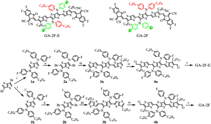
Based on the aforementioned considerations, we have successfully designed and synthesized two isomers of NFREAs, GA-2F-E and GA-2F, with their structures illustrated in Scheme 1. Both of these NFREAs exhibit asymmetric structures, differing solely in the positioning of fluorine substituents on their side chains. Specifically, they possess a core structure of thieno[3,2-b]thiophene, yet GA-2F-E bears two (4-butylphenyl)-N-(4-fluorophenyl)amino side chains, whereas GA-2F features one bis(4-fluorophenyl)amino and one bis(4-butylphenyl)amino side chain. We have conducted comprehensive investigations into the impact of fluorine substituent positioning on the photovoltaic performance, aggregation behaviors, and overall device efficiencies of these acceptors. The findings reveal that both GA-2F-E and GA-2F possess broad absorptions, spanning wavelengths from 450 nm to 880 nm. Notably, GA-2F-E demonstrates enhanced characteristics, including more compact π-π stacking, reduced bimolecular recombination, more efficient exciton transport, and higher, more balanced mobility. Consequently, the optimized D18:GA-2F-E-based OSC achieves a remarkable PCE of 16.45%, surpassing the 15.83% PCE of its D18:GA-2F counterpart. Our study underscores the significant potential of simple NFREAs in forthcoming applications and sheds light on the crucial role of fluorine substituent positioning in the design of more efficient NFREAs and the fabrication of high-performance OSCs.
Scheme 1
Scheme 1.
Chemical structures and synthetic routes of GA-2F-E and GA-2F. Reagents and conditions: (ⅰ) 4–Butyl–N-(4-fluorophenyl)aniline or bis(4-fluorophenyl)amine, bis(4-butylphenyl)amine, Pd(OAc)2, NaOt-Bu, P(t-Bu)3, o-xylene, 145 ℃; (ⅱ) NBS, DMF, 0 ℃; (ⅲ) trimethyl(6-octylthieno[3,2-b]thiophen-2-yl)stannane, Pd(PPh3)4, toluene, 110 ℃; (ⅳ) POCl3, 1,2-dichloroethane, DMF, 80 ℃; (ⅴ) 2-(5,6-difluoro-3-oxo-2,3-dihydro-1H-inden-1-ylidene)malononitrile, pyridine, CHCl3, r.t.
Scheme 1 outlines the synthetic routes for GA-2F-E and GA-2F. Starting materials 3,6-dibromothieno[3,2-b]thiophene, 4–butyl–N-(4-fluorophenyl)aniline, and bis(4-fluorophenyl)amine are commercially available, while bis(4-butylphenyl)amine is synthesized based on established literature procedures. At 145 ℃, using o-xylene as the solvent and Pd(OAc)2 as the catalyst, we achieved compound 1a in a yield of 77% through the Buchwald-Hartwig coupling of 3,6-dibromothieno[3,2-b]thiophene with diphenylamine. Subsequently, compound 1a was brominated using NBS in DMF at 0 ℃, resulting in a 96% yield of compound 2a. Next, compound 3a was synthesized via the Stille coupling between compound 2a and trimethyl(6-octylthieno[3,2-b]thiophen-2-yl)stannane, utilizing Pd(PPh3)4 as the catalyst precursor. Compound 4a was then obtained through the Vilsmeier-Haack reaction of compound 3a, achieving an 82% yield. Finally, the target compound GA-2F-E was synthesized via the Knoevenagel condensation reaction of compound 4a with 3-(1,1-dicyanomethylene)-5,6-difluoro-1-indanone, resulting in an 89% yield. GA-2F was also synthesized following the same procedure as GA-2F-E. Notably, both GA-2F-E and GA-2F demonstrate excellent solubility in commonly used organic solvents. Detailed synthetic procedures, along with 1H and 13C NMR spectroscopy data and mass spectrometry results for GA-2F-E and GA-2F, are provided in Supporting information.
Based on density functional theory (DFT), we conducted theoretical simulations to calculate the dipole moments of diphenylamine moieties within two NFREAs. As illustrated in Fig. 1a, there exists a notable disparity in the dipole moments of 4-butylaniline and 4-fluoroaniline, measured at 1.76 Debye and 3.55 Debye, respectively. Regarding (4-butylphenyl)-N-(4-fluorophenyl)amine, bis(4-fluorophenyl)amine, and bis(4-butylphenyl)amine, their respective dipole moments are calculated to be 2.26, 2.05, and 0.68 Debye, respectively. Notably, the asymmetric (4-butylphenyl)-N-(4-fluorophenyl)amino demonstrates the highest dipole moment. Additionally, Fig. 1b reveals distinct variations in the electrostatic potential (ESP) [46] distribution between GA-2F-E and GA-2F: From the perspective of the figure, it can be seen that two side chains of GA-2F-E have high electrostatic potential regions with electron donating ability (red part) and low electrostatic potential regions with electron withdrawing ability (blue part); as for GA-2F, the side chains either only has low electrostatic potential region (upper part), or only has high electrostatic potential region underneath, these disparities have potential implications for intermolecular stacking configurations and charge transport properties. Moreover, the uneven distribution of potentials along fluorinated aromatic substituents may influence charge separation mechanisms among NFREAs.
Figure 1
Figure 1.
(a) Molecular structures and dipole moments among 4-fluoroaniline, 4-butylaniline, bis(4-fluorophenyl) amine, 4–butyl–N-(4-fluorophenyl) aniline and bis(4-butylphenyl)amine. (b) ESP figures of GA-2F-E and GA-2F.
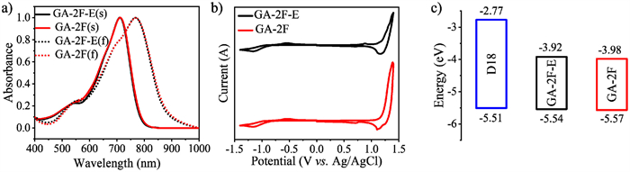
The UV–vis absorption spectra of GA-2F-E and GA-2F in chloroform solutions and as thin films are shown in Fig. 2a, with detailed optical parameters summarized in Table 1. As evident from Fig. 2a, the absorption spectra of GA-2F-E and GA-2F in chloroform solutions are nearly indistinguishable between 500 nm and 880 nm, exhibiting maximum absorption peaks at approximately 710 nm. In the thin film form, the absorption spectra of both acceptors exhibit broadening, and a notable red shift of approximately 50 nm in the absorption peaks relative to their solution counterparts, suggestive of J-aggregation formation. The maximum molar extinction coefficient of GA-2F-E in the film is 1.15 × 105 cm−1, which is slightly higher than that of GA-2F (1.03 × 105 cm−1). By considering the absorption edges (λonest) of the films, which are 860 nm for GA-2F-E and 873 nm for GA-2F, the optical bandgaps (Egopt) [47,48] for GA-2F-E and GA-2F are determined to be 1.42 and 1.41 eV, respectively.
Figure 2
Figure 2.
(a) UV–vis absorption spectra of GA-2F-E and GA-2F in dilute chloroform solutions (s) and as thin films (f). (b) CV plots of the two acceptors measured in 0.1 mol/L Bu4NPF6 acetonitrile solution at a scan rate of 100 mV/s. (c) Energy level diagram of D18, GA-2F-E and GA-2F.
To investigate the electrochemical properties of GA-2F-E and GA-2F, cyclic voltammetry (CV) was conducted using a Pt wire counter electrode and an Ag/AgCl/Cl reference electrode, and the curves are shown in Fig. 2b. From the onset oxidation and reduction potentials revealed by the CV curves, the highest occupied molecular orbital (HOMO) and lowest unoccupied molecular orbital (LUMO) energy levels were determined to be −5.54/−3.92 eV for GA-2F-E and −5.57/−3.98 eV for GA-2F, according to the equation EHOMO/LUMO = −e[Eox/red + 4.80 − EFc/Fc+]. Obviously, changing the fluorination position on the diphenylamino flanking groups has an impact on the energy levels of the two acceptors. The slightly higher LUMO energy level of GA-2F-E would provide a higher Voc for devices (vide infra). The detailed optical and electrochemical data for GA-2F-E and GA-2F are also summarized in Table 1. The energy level diagram for the polymer donor D18 and acceptors are shown in Fig. 2c.
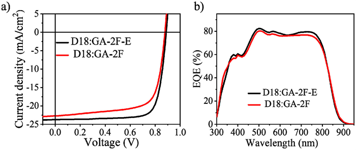
In order to evaluate the effect of fluorination positions on the photovoltaic properties of GA-2F-E and GA-2F, conventional OSCs with a device structure of indium tin oxide (ITO)/poly(3,4-ethylenedioxythiophene):polystyrene sulfonate (PEDOT:PSS)/active layer/PDINN/Ag were fabricated. Referring to previous studies with similar acceptor structures, D18 was selected as the polymer donor to pair with these two acceptors [1,6,45]. The device fabrication conditions, including the active layer composition (D:A weight ratio), additive content, and thermal annealing temperature, are carefully optimized. The detailed photovoltaic data are summarized in Table 2 and the J-V curves are shown in Fig. 3a. The optimized D:A weight ratio was 1:1.2. The additive was TT-Cl (4 mg/mL), and the thermal annealing temperature was 100 ℃ (Tables S1-S4 in Supporting information). Both devices show higher PCE than D18:2BTh-2F [30] based device, where 2BTh-2F owns the same structure except for the fluorination on side chains. The D18:GA-2F-based device shows a PCE of 15.83% with an open-circuit voltage (Voc) of 0.889 V, a short-circuit current (Jsc) of 23.21 mA/cm2, and a fill factor (FF) of 76.55%. In contrast, D18:GA-2F-E-based devices show a higher PCE of 16.45% with an enhanced Voc of 0.890 V, a comparable Jsc of 23.71 mA/cm2, and an FF of 78.15%. The higher Voc of D18:GA-2F-E-based devices can be attributed to the higher LUMO level of GA-2F-E compared to that of GA-2F. The external quantum efficiency (EQE) spectra of the optimal devices were measured to confirm the accuracy of Jsc values determined by the J-V measurements. As shown in Fig. 3b, the maximum EQE reached about 80% from 300 nm to 900 nm for both GA-2F-E and GA-2F-based devices. The Jsc values, calculated by integrating the EQE curves, are all within a 5% difference compared to those obtained from the J-V measurements.
Table 2
Table 2.
Photovoltaic parameters of GA-2F-E and GA-2F based devices.
To understand the charge carrier dynamic process in the GA-2F-E and GA-2F-based devices, the charge generation, transport, and recombination are investigated. The dependence of photocurrent density (Jph) on effective voltage (Veff) is measured to analyze the exciton dissociation process of OSCs as shown in Fig. S1a (Supporting information). The exciton dissociation efficiency (Pdiss) is determined from the ratio of Jph/Jsat, where Jsat is the abbreviation for saturation current density. Under short-circuit conditions, Pdiss values are 98% and 97% for the GA-2F-E and GA-2F-based devices, respectively, which indicates that GA-2F-E-based devices have a higher exciton dissociation efficiency. Besides, the light intensity (Plight), which is closely related to Jsc, is measured to explore the charge recombination properties. In theory, the relation between Jsc and Plight follows the expression, Jsc∝Plightα. When α is very close to 1, bimolecular recombination process in the device is negligible. As shown in Fig. S1b (Supporting information), the α values of GA-2F-E and GA-2F-based devices are 0.965 and 0.961, indicating less bimolecular recombination occurred in the GA-2F-E-based device. Therefore, higher exciton dissociation efficiency and less bimolecular recombination are consistent with the comparable Jsc and higher FF values obtained from the GA-2F-E-based devices. Furthermore, the relationship between the Voc and Plight, described as Voc ∝ n(kT/q)ln(Plight), where k, T, and q represent the Boltzmann constant, temperature in Kelvin, and elementary charge, respectively, was evaluated to study the trap-assisted recombination. As shown in Fig. S1c (Supporting information), the n values of the GA-2F-E and GA-2F-based devices are 1.03 and 1.04, respectively, indicating that trap-assisted recombination is effectively suppressed for both GA-2F-E and GA-2F-based devices.
To study the energy loss (Eloss) in the GA-2F-E and GA-2F-based devices, the charge transfer state energy (Ect) from the electroluminescence (EL) and highly sensitive external quantum efficiency (sEQE) were measured to calculate the Eloss of the photovoltaic devices. According to the equation [49]: Eloss = Eg – qVoc, where Eg is estimated from the intersection of the optical absorption and photoluminescence curves of the low band gap acceptors (Table 3), the Eloss values for GA-2F-E and GA-2F-based OSCs are 0.605 and 0.600 eV, respectively, with an almost negligible difference. From the EL and sEQE spectra (Fig. S2 in Supporting information), the Ect values of GA-2F-E and GA-2F-based devices are 1.43 and 1.42 eV, respectively. We can further divide Eloss into three parts: charge generation energy loss (ΔEct = Eg − Ect), non-radiative recombination energy loss (∆Enr) and radiative recombination energy loss (∆Er). GA-2F-E-based devices display a ΔEct of 0.067 eV, which is close to that of GA-2F (0.063 eV). Additionally, ∆Enr of the GA-2F-E-based device is calculated to be 0.258 eV from the EQE of electroluminescence (EQEEL) via the equation: ΔEnr = −kTln(EQEEL), which is slightly lower than that of GA-2F-based devices (0.262 eV) (Fig. S3 in Supporting information). According to ∆Er = Eloss – ∆Enr, ∆Er values for devices based on GA-2F-E and GA-2F are calculated to be 0.264 eV and 0.260 eV, respectively. The detailed parameters of energy loss are presented in Table 3.
Table 3
Table 3.
Detailed Eloss of GA-2F-E and GA-2F based devices.
To examine the charge transport properties of devices based on GA-2F-E and GA-2F, the space-charge-limited current method was utilized. The hole (μh) and electron (μe) transport mobilities were estimated with typical device structures of ITO/PEDOT:PSS/active layer/Au and ITO/ZnO/active layer/Al, respectively. As shown in Fig. S4 and Table S5 (Supporting information), the μh and μe values are 7.39 × 10⁻⁴ cm2 V−1 s−1 and 7.18 × 10⁻⁴ cm2 V−1 s−1 for D18:GA-2F-E-based devices, and 6.07 × 10⁻⁴ cm2 V−1 s−1 and 6.82 × 10⁻⁴ cm2 V−1 s−1 for D18:GA-2F-based devices, respectively. These results demonstrate that the different fluorinated positions at the side chains of the acceptors can influence the charge transport mobility of their blend films with polymer donors. Furthermore, D18:GA-2F-E-based devices possess a more balanced μh/μe ratio (1.03) compared to D18:GA-2F-based ones (0.88). These results provide a clear explanation for the superior Jsc and FF values of D18:GA-2F-E-based devices.
Atomic force microscope (AFM) and transmission electron microscope (TEM) are used to investigate the surface and the bulk morphology of the blend films (Fig. S5 in Supporting information). As shown in Figs. S5a and d, the D18:GA-2F-E and D18:GA-2F-based blend films display homogenous morphology, and the D18:GA-2F-E-based blend film shows a higher root mean square (RMS) roughness value of 0.917 nm than that of 0.808 nm for the D18:GA-2F-based blend film, which might be attributed to the improved crystallinity of GA-2F-E. According to the TEM images, obvious fiber-like structures can be observed in both the D18:GA-2F-E and D18:GA-2F films, which is conducive to achieving a high FF value with efficient charge separation and transport. Particularly, some thicker fiber-like structures can be observed in the D18:GA-2F-E-based blend films, which might be part of the reason for its higher Jsc and FF than those of the D18:GA-2F-based devices. The TEM results are well consistent with those from the AFM measurements.
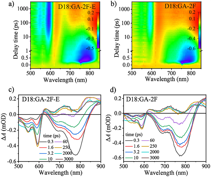
To gain deeper insight into the charge transfer of binary devices, femtosecond-transient absorption (fs-TA) spectra of the blend films were measured and the charge transfer kinetics of devices were studied. To selectively excite the acceptors in blend films, a low pump pulse with a wavelength of 760 nm and an intensity of 0.13 µJ/cm2 was implemented. The resulting TA spectra are presented as 2D color plots, and several representative TA spectra were selected at specific delay times to facilitate an intuitive comparison between two blend films. As shown in Fig. 4, two new bleaching peaks appeared at 545 and 590 nm in the donor absorption region. The peak intensity of D18:GA-2F-E blend film is stronger than that of D18:GA-2F blend films, indicating more efficient hole transfer in D18:GA-2F-E blend film. To further reveal the exciton diffusion and dissociation process, the decay dynamics of the ground-state bleaching (GSB) signals (590 nm) are shown in Fig. S6 (Supporting information) and the time constants (τ) of the blend films are summarized in Table S6 (Supporting information), where τ1 and τ2 represent the rapid dissociation of excitons at the interface and the diffusion of the excitons within the domain, respectively. The τ1 and τ2 values are 1.12 ± 0.05 and 18.76 ± 0.44 ps for D18:GA-2F-E blend film, 1.80 ± 0.15 and 22.18 ± 2.06 ps for D18:GA-2F blend film, respectively. Shorter τ1 and τ2 indicate that the D18:GA-2F-E blend film has quicker exciton dissociation at the donor-acceptor interface and faster diffusion of excitons within GA-2F-E domain toward the interface prior to dissociation, which is also beneficial for charge generation and collection in OSCs.
Figure 4
Figure 4.
The TA color plot image and the corresponding TA spectra of (a, c) D18:GA-2F-E and (b, d) D18:GA-2F-based film with various decay times under 760 nm excitation.
We employed grazing-incidence wide-angle X-ray scattering (GIWAXS) technology to delve into the molecular packing, orientation, and aggregation states in pure and blend films. As shown in Fig. S7 (Supporting information), diffraction peaks in the out-of-plane (OOP) direction are clearly observable from the GIWAXS patterns of neat GA-2F-E and GA-2F films. This indicates the formation of a face-on orientation with short π-π stacking distances of 1.70 Å-1 (equivalent to 3.70 Å) for GA-2F-E and 1.66 Å-1 (equivalent to 3.79 Å) for GA-2F in the films, respectively. Using the Scherrer equation, CCL = 2π × 0.90/FWHM, we calculated the crystal coherence length (CCL) to analyze the molecular packing in the acceptor films. The results showed CCL values of 19.43 and 18.12 Å for the (010) diffraction in the OOP direction. This suggests that the GA-2F-E film exhibits higher crystalline quality with a shorter π-π stacking distance, facilitating efficient charge transport in the active layer. It is worth noting that the crystallinity difference between GA-2F-E and GA-2F may be attributed to enhanced intramolecular interactions due to varying fluorination positions on the side chain. For D18:GA-2F-E and D18:GA-2F blend films, the (010) diffraction peaks in the OOP direction are located at 1.72 and 1.68 Å-1, corresponding to π-π stacking distances of 3.65 Å and 3.74 Å, respectively. Additionally, the CCL values for the (010) diffraction in the OOP direction are calculated to be 23.46 and 22.22 Å for D18:GA-2F-E and D18:GA-2F, respectively (Table S7 in Supporting information). In conclusion, GA-2F-E-based blend films exhibit enhanced diffraction features in 2D patterns and stronger (100) and (010) diffraction peaks in 1D profiles. This indicates a more preferred face-on orientation and a higher degree of structural order in the D18:GA-2F-E blend film.
In this study, we designed and synthesized two isomeric NFREAs, namely GA-2F-E and GA-2F, with different fluorination positions in their side chains. We conducted an in-depth investigation into the effects of fluorination positions on the optoelectronic properties, aggregation behavior, and overall device performance of these acceptors. The experimental results revealed that both GA-2F-E and GA-2F possess a broad absorption band, spanning from 450 to 880 nm. Through GIWAXS characterization, we observed that GA-2F-E exhibits tighter π-π stacking, along with superior crystallinity and coherence length compared to GA-2F. Notably, the optimized OSCs based on D18:GA-2F-E achieved a remarkable PCE of 16.45%, surpassing the 15.83% PCE of devices utilizing D18:GA-2F. The enhanced photovoltaic performance of D18:GA-2F-E-based devices is primarily attributed to reduced bimolecular recombination, efficient exciton transport, and higher, well-balanced mobility.
Declaration of competing interest
The authors declare that they have no known competing financial interests or personal relationships that could have appeared to influence the work reported in this paper.
This work is financially supported by the National Natural Science Foundation of China (Nos. 22375024, 21975031, 51933001, and 21734009). A portion of this work is based on the data obtained at BSRF-1W1A. The authors gratefully acknowledge the cooperation of the beamline scientists at BSRF-1W1A beamline.
Supplementary materials
Supplementary material associated with this article can be found, in the online version, at doi:10.1016/j.cclet.2025.111622.
Figure 1
(a) Molecular structures and dipole moments among 4-fluoroaniline, 4-butylaniline, bis(4-fluorophenyl) amine, 4–butyl–N-(4-fluorophenyl) aniline and bis(4-butylphenyl)amine. (b) ESP figures of GA-2F-E and GA-2F.
Figure 2
(a) UV–vis absorption spectra of GA-2F-E and GA-2F in dilute chloroform solutions (s) and as thin films (f). (b) CV plots of the two acceptors measured in 0.1 mol/L Bu4NPF6 acetonitrile solution at a scan rate of 100 mV/s. (c) Energy level diagram of D18, GA-2F-E and GA-2F.
Figure 4
The TA color plot image and the corresponding TA spectra of (a, c) D18:GA-2F-E and (b, d) D18:GA-2F-based film with various decay times under 760 nm excitation.

 DownLoad:


 下载:
下载:


 下载:
下载:
