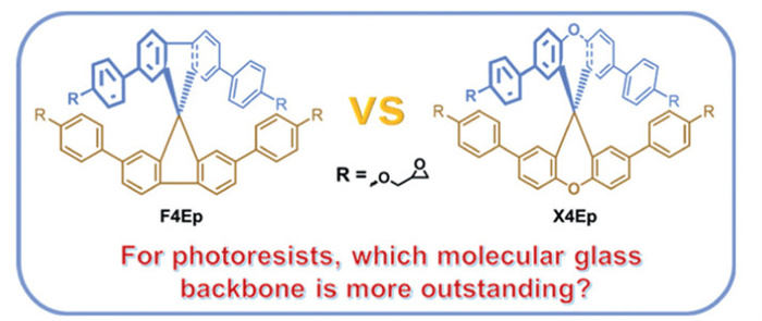
Figure 1.
The photoresists based on backbone spirobifluorene and spirobixanthene.
Spirobixanthene surpasses spirobifluorene as key backbone for molecular negative photoresists
Yu Yan , Chenfei Zhao , Jingwen Hui , Xinfu Zhang , Linlin Zhao , Lujia Yang , Zhipeng Ning , Pengzhong Chen , Lingcheng Chen , Xiaojun Peng , Yi Xiao

In the semiconductor manufacturing field, the number of transistors per unit area increases continuously as predicted by the well-known Moore's law [1]. To date, the process half pitch (HP) has been scaled down to sub-10 nm through tremendous advancements in advanced photolithography technology, particularly extreme ultraviolet lithography (EUVL) and electron-beam lithography (EBL).
Molecular glass resists (MGs) exhibit innate characteristics, including small molecular volume and monodispersity [2], which are extensively studied to address the trade-off between resolution and line edge roughness (LER) caused by the absence of chain entanglement and internal stress observed in polymeric resists [3-6]. The molecular backbone serves as the core architecture of MGs. High-performance backbones typically demonstrate the following features: (a) Rigidity ensures superior thermostability, elevated glass transition temperature (Tg), and robust mechanical properties; (b) A distorted spatial configuration enhances film-forming capability. Based on backbone variations, several representative MGs have been reported with unsatisfactory performances. For example, calixarene-based negative-tone MG exhibits limited resolution and significant LER [7], while positive-tone calixarene MG show reduced Tg upon t-Boc deprotection [8]. t-Boc-protected polyphenol-based positive-tone MGs suffer from low Tg [9]. Noria-based MGs demonstrate poor film-forming properties due to crystallization tendencies [10]. Bisphenol A-derivative epoxy negative resist displays pronounced bridging defects without photodegradable nucleophiles [11]. And adamantane-based positive-tone MGs present low Tg [12] and substantial LER [13]. Therefore, there still remains scope to develop novel high-performance backbone architectures for MGs.
Yang et al. previously developed a positive-tone photoresist utilizing spirobifluorene backbone with rigid spiral structure, demonstrating an improved resolution lithography [14].
In this work, spirobixanthene is chosen as the backbone of MG for the first time, with the epoxy-based negative photoresist X4Ep as the example to illustrate the superiority of this new backbone. The high rigidity and twisted spiral structure of spirobixanthene, through restricting rotational freedom, endues X4Ep dense amorphous film morphology with very high Tg. For comparative analysis, the spirobifluorene-based negative photoresist F4Ep was also synthesized, as illustrated in Fig. 1. Compared to positive-tone photoresists, negative-tone variants demonstrate superior etching and chemical corrosion resistance due to their crosslinked networks, while simultaneously maintaining enhanced pattern integrity against structural collapse.
X4Ep exhibits excellent amorphous characteristics attributed to the asymmetry of its distorted xanthene units, where the incomplete perpendicularity of these xanthene moieties effectively suppresses intermolecular crystallization tendencies. In contrast, the fully perpendicular fluorene components in F4Ep promote intermolecular crystalline stacking, which aggravates uneven photoacid generator (PAG) distribution and non-uniform acid diffusion [15]. This phenomenon ultimately leads to increased LER and bridging defects in patterned features due to inconsistent acid-catalyzed crosslinking. Significantly, crystallization analyses and EBL conclusively demonstrate that X4Ep delivers superior performance compared to F4Ep.
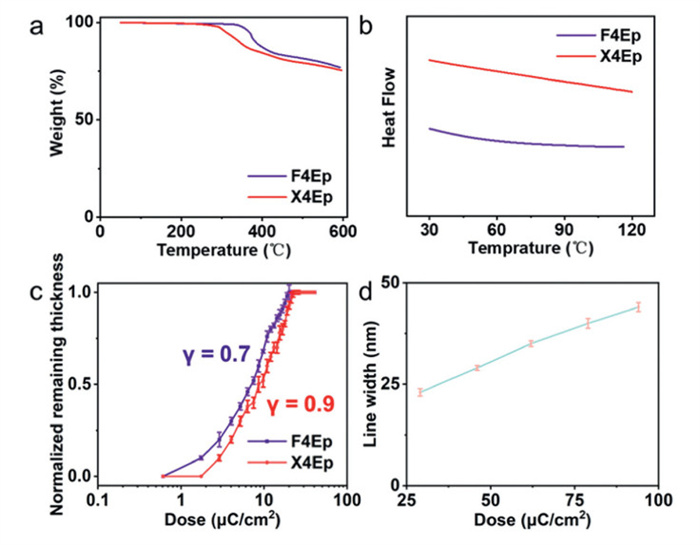
Next, we conducted a systematic comparison between X4Ep and F4Ep. Thermal characteristics constitute critical performance parameters for photoresist materials. For epoxy-based photoresists, both thermal crosslinking temperature and Tg dictate the upper operational limits for post-apply bake (PAB) and post-exposure bake (PEB) in lithographic processing. As shown in Figs. 2a and b, and Table S1 (Supporting information), the thermo-gravimetric analysis (TGA) profiles reveal distinct thermal behaviors: F4Ep demonstrates initial weight loss onset at 325 ℃, with its 5% decomposition temperature (Td, 5%) reaching 368 ℃. X4Ep maintains no observable weight loss until 245 ℃ with a Td, 5% of 310 ℃. In fact, these Td values represent the thermal decomposition temperatures of the crosslinked polymer networks. Thin-layer chromatography monitoring confirmed powder stability across temperature gradients, indicating an optimal thermal crosslinking temperature around 130 ℃. Differential scanning calorimetry (DSC) analysis showed no detectable Tg within the tested range, suggesting exceptional resistance to thermal deformation. Collectively, these thermal analyses confirm that both F4Ep and X4Ep satisfy the stringent thermal requirements for advanced lithographic applications.
Following successful exposure, the developer directly determines the formation of lithography patterns. Solubility profiles in different solvents are depicted in Table S2 (Supporting information) at room temperature; specifically, X4Ep exhibits favorable solubility in organic solvents including 1-methoxy-2-propyl acetate (PGMEA), cyclopentanone, ethyl lactate (EL), and 4-methyl-2-pentanone (MIBK). Notably, F4Ep is insoluble in PGMEA, while both compounds demonstrate limited solubility in hexane, 1-methoxy-2-propanol (PGME), and isopropyl alcohol (IPA). Consistent with prior research [11,16], development using MIBK enables the formation of lithography patterns.
For low molecular-weight organic molecules, the amorphous molecular state constitutes a prerequisite for forming smooth films and low LER patterns. Crystallization exacerbates the uneven distribution of PAGs and induces inhomogeneous acid diffusion, resulting in differential chemical reaction degrees within exposed regions. This phenomenon ultimately compromises resolution performance and amplifies LER [10,15,17-19].
X-ray diffraction (XRD) characterization was conducted to evaluate the amorphous states of F4Ep and X4Ep under ambient conditions. As demonstrated in Fig. 3a, F4Ep exhibits multiple sharp diffraction peaks within the 15°–35° range, indicative of partial crystallization, with the maximum peak intensity occurring at 2θ = 20.2°. In contrast, X4Ep displays a broad smooth peak across the same angular range, confirming its predominantly amorphous nature. The observed maximum peak intensity at 2θ = 19.7°, combined with the featureless diffraction profile, suggests that X4Ep maintains superior amorphous characteristics compared to F4Ep. This enhanced amorphous state predicts improved film smoothness and reduced LER in lithographic applications.
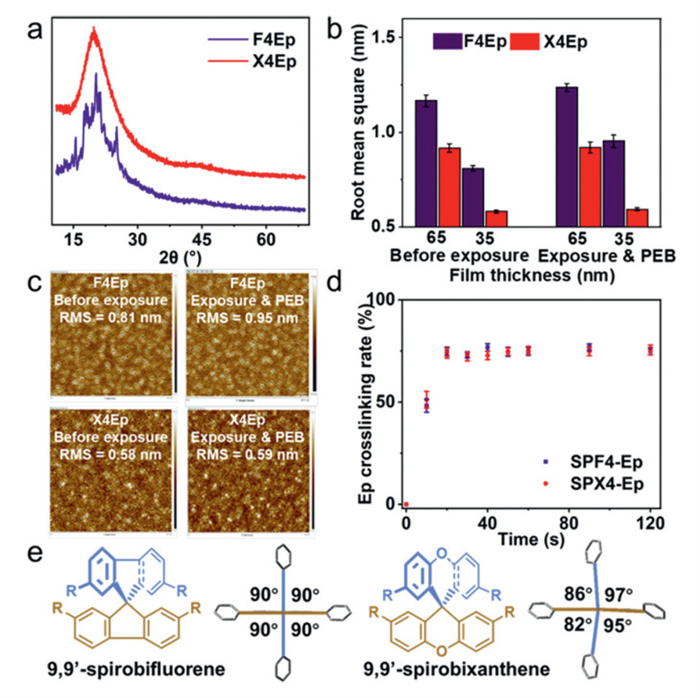
Atomic force microscope (AFM) was employed to characterize the 65 and 35 nm film surface roughness of F4Ep and X4Ep on silicon wafers, with root mean square (RMS) roughness quantified in 50 µm × 50 µm scan areas. X4Ep exhibits superior surface planarity compared to F4Ep at equivalent thicknesses, while both systems demonstrate progressive RMS reduction accompanying film thickness decreases from 65 nm to 35 nm (Figs. 3b and c). Pre- versus post-exposure surface roughness analysis reveals stress evolution throughout the wafer, at 35 nm thickness, epoxy crosslinking in F4Ep induces a pronounced 0.14 nm RMS increase from 0.81 nm to 0.95 nm, whereas X4Ep maintains surface roughness virtually unaltered (ΔRMS = 0.01 nm) post-processing (Fig. 3c). Fourier-transform infrared spectroscopy (FTIR) kinetic monitoring during 90 ℃ PEB demonstrates comparable crosslinking rates (75% conversion at 60 s) between materials (Fig. 3d and Table S3 in Supporting information). This parity implies roughness variations originate from backbone structural disparities rather than crosslinking efficiency. Specifically, F4Ep's partial crystallinity exacerbates spatial heterogeneity in PAG distribution and acid diffusion uniformity, generating regional crosslink density gradients. These intrinsic stress differentials propagate surface deformation manifesting as elevated RMS values.
Density functional theory (DFT) calculations provide mechanistic insights into the divergent film-forming characteristics and surface roughness, as illustrated in Fig. 3e. The structural distinction resides exclusively in the backbone configurations of F4Ep versus X4Ep. The sp3-hybridized spiroconjugated carbons in spirobifluorene induce severe interplanar distortion, forcing complete orthogonality (90° dihedral angle) between the two aromatic planes. This rigid symmetry accounts for partial crystallization in F4Ep. Conversely, the oxygen-bridged xanthene units in spirobixanthene impose conformational constraints, generating four distinct dihedral angles (96°, 95°, 87°, and 82°) through non-coplanar deformation. Such inherent molecular asymmetry suppresses crystalline ordering, thereby stabilizing a homogeneous amorphous phase that enables uniform PAG distribution and consistent acid diffusion. These computational findings align with experimental observations: XRD-determined amorphous state differences and stress-induced roughness evolution post-exposure.
Systematic evaluation of film thickness variation versus exposure dose provides critical insights for optimizing line/space (L/S) pattern fabrication. A 6 × 6 array of 2 µm × 2 µm test patterns was e-beam exposed with doses spanning 0–40 µC/cm2, followed by PEB at 90 ℃ for 60 s and development using MIBK for 30 s. AFM profilometry revealed dose-dependent thickness retention, demonstrating progressive film thickness increase with escalating exposure dose (Fig. 2c).
Notably, F4Ep and X4Ep exhibit comparable photosensitivity, with 100% thickness retention doses (D100) of 20 and 23 µC/cm2, respectively. Lithographic contrast (γ) values calculated through normalized thickness-dose curves yielded γ = 0.7 for F4Ep versus γ = 0.9 for X4Ep. This sub-optimal contrast compared to commercial positive-tone resist EUV-2D (γ > 2) [20] stems from compromised acid diffusion control - while base additives enhance contrast via acid neutralization, they concomitantly suppress sensitivity [21]. EUV-2D's performance benefits from optimized base quencher formulation achieving balanced diffusion-restriction.
Comparative lithographic evaluation of F4Ep versus X4Ep for 50 and 35 nm HP L/S patterning revealed fundamental performance disparities. F4Ep consistently exhibited bridge defects and pattern collapse in dense L/S configurations (Figs. 4a and b, Fig. S3 in Supporting information), with irremediable failure persisting despite EBL parameter optimization and process condition iterations. Conversely, X4Ep achieved defect-free patterning with sub-5 nm edge acuity across all test structures (Figs. 4c and d).
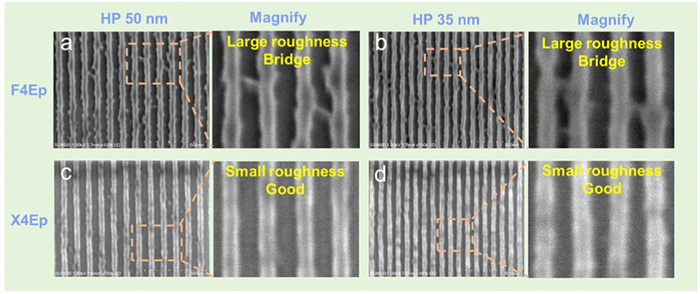
This dichotomy originates from backbone structural divergence: X4Ep's conformational asymmetry enables uniform epoxy crosslinking via spatially homogeneous PAG distribution and controlled acid diffusion (Fig. 3e). Such molecular-level uniformity translates to superior lithographic fidelity compared to both F4Ep and state-of-the-art hyperbranched epoxy-based molecular glasses BPA-6Ep (bridge formation [11]) and 3Ep/4Ep (large LER [22]) (Fig. S2 in Supporting information). These flexible backbone systems may undergo stress-induced deformation during crosslinking, whereas X4Ep's rigid spiroconjugated architecture effectively suppresses dimensional instability. Given these compelling performance advantages, subsequent investigations focused exclusively on X4Ep systems.
Lithographic patterning fidelity was assessed via 50 nm HP L/S fabrication with dose-dependent dimension control. Quantitative evaluation of dose-linewidth correlation was performed through dose sweeps spanning 29–94 µC/cm2 (Fig. 2d). Cross-sectional scanning electron microscope (SEM) micrographs presented in Fig. S4 (Supporting information) demonstrate linear development behavior, revealing a well-defined linear proportionality between exposure dose and printed feature dimensions (23–44 nm linewidth over 29–94 µC/cm2 range).
This predictable behavior stems from acid-catalyzed epoxy crosslinking kinetics: Elevated doses activate increased PAG triphenylsulfoniumperfluoro-1-butanesufonate (TPS-PFBS) decomposition, thereby accelerating proton-mediated crosslinking governed by acid diffusion gradients. Importantly, continuous line formation was achieved with complete pattern fidelity, confirming absence of bridging defects across the operational dose window.
The dimensional resolution of L/S patterns is constrained by exposure dose, with film thickness serving as a critical factor in achieving high-quality nanoscale HP patterns [23,24]. As demonstrated in Figs. 5a and b, distinct pattern collapse phenomena were observed in the 65 nm film, whereas the 35 nm film exhibited no detectable structural deformations. This thickness-dependent behavior is attributed to two primary mechanisms: capillary forces between pattern sidewalls during the development process [25] and stochastic defect formation [26].
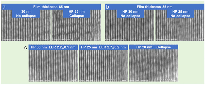
Notably, the 65 nm film possesses a higher aspect ratio compared to the 35 nm counterpart. Since capillary forces exhibit inverse proportionality to aspect ratio, the thicker film experiences significantly greater mechanical stress during solvent evaporation. Consequently, pattern collapse incidents occur preferentially in thicker films under equivalent processing conditions.
A systematic investigation of the correlations between exposure dose, film thickness, and pattern resolution was conducted. Successful fabrication of high-density L/S patterns was achieved, demonstrating 30 nm HP structures with 2.2 nm LER and 25 nm HP patterns exhibiting 2.7 nm LER, as documented in Fig. 5c. Unfortunately, structural collapse phenomena were observed in 20 nm HP L/S configurations, indicating a critical resolution threshold under the implemented processing conditions.
Conclusively, a novel epoxy-based molecular glass negative-tone photoresist X4Ep featuring a rigid spirobixanthene backbone was successfully designed and synthesized. Both F4Ep and X4Ep demonstrated high thermal stability, with no detectable Tg observed prior to thermal crosslinking. XRD analysis combined with theoretical calculations revealed enhanced amorphous stacking characteristics in X4Ep, significantly surpassing those of F4Ep. These observations position X4Ep as a superior candidate for advanced photoresist applications.
EBL revealed persistent bridging and collapse defects in F4Ep even with optimized exposure parameters and process conditions, attributed to non-uniform epoxy crosslinking resulting from PAG aggregation and acid diffusion anomalies induced by partial crystallization in F4Ep's symmetrical molecular structure. In contrast, X4Ep exhibited exceptional lithographic performance, demonstrating high sensitivity with a dose-to-clear (D100) of 23 µC/cm2 while maintaining structural integrity without bridging or collapse phenomena.
The lithographic capabilities were further validated through successful fabrication of high-density L/S patterns, achieving 30 nm HP features with 2.2 nm LER and 25 nm HP patterns demonstrating 2.7 nm LER. This systematic investigation established a robust paradigm for epoxy-based molecular glass negative-tone photoresist development while substantiating the spirobixanthene architecture as a highly promising molecular framework for advanced photoresist design.
The authors declare that they have no known competing financial interests or personal relationships that could have appeared to influence the work reported in this paper.
Yu Yan: Writing – review & editing, Writing – original draft, Visualization, Validation, Project administration, Methodology, Investigation, Formal analysis, Data curation, Conceptualization. Chenfei Zhao: Validation. Jingwen Hui: Validation. Xinfu Zhang: Supervision, Resources, Funding acquisition. Linlin Zhao: Validation. Lujia Yang: Software. Zhipeng Ning: Validation. Pengzhong Chen: Resources. Lingcheng Chen: Supervision. Xiaojun Peng: Writing – review & editing, Resources. Yi Xiao: Writing – review & editing, Writing – original draft, Supervision, Resources, Project administration, Methodology, Funding acquisition.
This work was supported by the National Natural Science Foundation of China (Nos. 22278059, 22174009, 22078047), Fundamental Research Funds for the Central Universities (Nos. DUT24ZD119, DUT22LAB601, DUT22LAB608).
Supplementary material associated with this article can be found, in the online version, at doi:
F. Schwierz, J. Pezoldt, R. Granzner, Nanoscale 7 (2015) 8261–8283.
A. De Silva, N.M. Felix, C.K. Ober, Adv. Mater. 20 (2008) 3355–3361. doi: 10.1002/adma.200800763
T. Nishikubo, H. Kudo, J. Photopolym. Sci. Technol. 24 (2011) 9–18. doi: 10.2494/photopolymer.24.9
Y. Chen, L. Li, G. Han, et al., Chin. Chem. Lett. 36 (2025) 110458. doi: 10.1016/j.cclet.2024.110458
S.W. Zhou, C. Yu, M. Chen, et al., Smart Mol. 1 (2023) e20220009. doi: 10.1002/smo.20220009
Y. Peng, P. Chen, H. Chen, et al., Smart Mol. 3 (2025) e20240043. doi: 10.1002/smo.20240043
H. Oizumi, T. Kumise, T. Itani, J. Photopolym. Sci. Technol. 21 (2008) 443–449. doi: 10.2494/photopolymer.21.443
S. Kang, W. l. Wu, K.W. Choi, et al., Macromolecules 43 (2010) 4275–4286. doi: 10.1021/ma902548a
N.M. Felix, A. De Silva, C.M.Y. Luk, et al., J. Mater. Chem. 17 (2007) 4598–4604. doi: 10.1039/b709649f
H. Seki, H. Kudo, H. Oizumi, et al., Jpn. J. Appl. Phys. 50 (2011) 121602. doi: 10.1143/JJAP.50.121602
J. Gao, S. Zhang, X. Cui, et al., Adv. Mater. Interfaces 10 (2023) 2300194. doi: 10.1002/admi.202300194
S. Hu, J. Chen, T. Yu, et al., J. Mater. Chem. C 10 (2022) 9858–9866. doi: 10.1039/d2tc01339h
S. Hu, J. Chen, T. Yu, et al., Chem. Res. Chin. Univ. 39 (2022) 139–143.
J. Chen, Q. Hao, S. Wang, et al., ACS Appl. Polym. Mater. 1 (2019) 526–534.
Y. Shirota, J. Mater. Chem. 10 (2000) 1–25.
D.L. Olynick, P.D. Ashby, M.D. Lewis, et al., J. Polym. Sci. Part B: Polym. Phys. 47 (2009) 2091–2105. doi: 10.1002/polb.21806
H. Lee, S. Park, M. Kim, et al., J. Mater. Chem. C 9 (2021) 1183–1195. doi: 10.1039/d0tc04104a
B.P. Prajwal, J.M. Blackwell, P. Theofanis, et al., Chem. Mater. 35 (2023) 9050–9063. doi: 10.1021/acs.chemmater.3c01750
Z. Wang, H. Du, H. Xin, et al., Chem. Mater. 36 (2024) 10841–10849. doi: 10.1021/acs.chemmater.4c02731
R.S. Mackay, Emerging Lithographic Technologies Ⅷ, SPIE, Santa Clara, California, 2004.
J.L. Sturtevant, Advances in Resist Technology and Processing XXI, SPIE, Santa Clara, California, 2004.
T.I. Wallow, C.K. Hohle, Advances in Patterning Materials and Processes XXXII, SPIE, San Jose, California, 2015.
J.L. Sturtevant, Advances in Resist Technology and Processing XXII, SPIE, San Jose, California, 2005.
J.W. Thackeray, J. Micro Nanolithogr. MEMS MOEMS 10 (2011) 033009. doi: 10.1117/1.3616067
S.F. Chini, A. Amirfazli, Langmuir 26 (2010) 13707–13714. doi: 10.1021/la101521k
P.P. Naulleau, Extreme Ultraviolet (EUV) Lithography Ⅳ, SPIE, San Jose, California, 2013.

Figure 2 Basic thermal and exposure properties. (a) TGA profiles. (b) DSC profiles. (c) Normalized remaining thickness of resists at different exposure. (d) Variation curve of line width for 50 nm HP L/S patterns at different dose of X4Ep. Film thickness: 65 ± 5 nm. Mean ± SD (n = 3).

Figure 3 The properties of film. (a) XRD profiles. (b) RMS changes of film before and after exposure and PEB. (c) AFM images, film thickness: 35 ± 3 nm. (d) Epoxy crosslinking efficiency during PEB at 90 ℃. (e) Symmetry analysis by DFT calculation. Mean ± SD (n = 3).

Figure 4 The film thickness behavior and lithography performance of F4Ep and X4Ep. (a–d) SEM images of HP 50 nm and 35 nm L/S patterns. Dose: F4Ep 30 µC/cm2, X4Ep 49 µC/cm2. Film thickness: 65 ± 5 nm.

 扫一扫看文章

扫一扫关注我们
 DownLoad:

 下载:
下载:

 下载:
下载: