Received Date:
10 January 2025 Accepted Date:
12 March 2025 Revised Date:
06 March 2025 Available Online:
15 July 2026
Abstract:
perovskite solar cells have attained exceptional power conversion efficiencies, offering a robust material foundation and device design process for the future of photovoltaics. In addition to optimizing perovskite materials for charge-related properties, it is essential to consider spin-related characteristics, as these could prove to be a pivotal factor in enhancing the photoelectric conversion efficiency. In this study, perovskite solar cells featuring various perovskite/transport layer interfaces were engineered to investigate the interfacial spin polarization’s impact on charge extraction. The intensity of charge extraction correlates directly with the interfacial spin polarization. By applying an external electric field, the interfacial spin polarization can be further amplified, thereby enhancing charge extraction. This amplified charge extraction, resulting from increased interfacial spin polarization, can substantially boost the overall photocurrent, thus enabling a high power conversion efficiency.
The significance of renewable energy has been increasingly acknowledged in recent years, as the global community faces various challenges. Hybrid organic-inorganic perovskites have emerged as promising photovoltaic materials, owing to their exceptional optoelectronic properties and the feasibility of high-throughput manufacturing of perovskite solar cells [1-5]. The power conversion efficiency of perovskite solar cells has rapidly escalated, soaring from less than ten percent to over 26% [6-8], positioning them as a highly regarded contender for the next generation of photovoltaic devices. High-performance perovskite solar cells (PSCs) typically feature a sandwich-like architecture, consisting of a perovskite absorber layer that is sandwiched between an electron-transporting material (ETM) and an organic hole-transporting material (HTM). The majority of high-efficiency devices are based on the modification of perovskite layers [9,10] or improvement of transport materials [11-13]. The incorporation of an excess amount of lead iodide proves advantageous in diminishing halide vacancy concentration and elevating perovskite crystallization [14]. An ammonium salt of amidinopyrimidine hydrochloride is introduced into the wet perovskite film for modulating the charged traps [15]. In addition, ETMs and HTMs are further developed to improve compatibility with dopants and energy levels matching those of perovskite [16].
In addition to enhancements in the perovskite layer and the transport layer, the interaction between these two layers is also a critical factor influencing the overall photovoltaic performance [17-20]. Pentylammonium acetate was introduced into the interface between perovskite and hole transport layer to fabricate highly efficient and stable flexible PSCs [21]. The organometallic compound ferrocenyl-bis-thiophene-2-carboxylate not only offers robust chemical Pb-O binding to diminish surface trap states but also enhances interfacial electron transfer [22]. Prototypical polymers were adopted to investigate the effects of the molecular structure of polymeric passivating agents on the effectiveness of surface defect passivation [23,24]. Recently, a surface sulfidation treated perovskites exhibited a shallow Fermi level, which induced an extra back-surface field at the perovskite interface through band bending [25], an unwanted resistive barrier between the perovskite and the electron transport layer can be overcome to increase PCE [26-28]. Therefore, it is important to recognize that the interfacial engineering between the perovskite layer and the transport layer significantly enhances our comprehension of the high photovoltaic performance. However, besides modifying interfacial passivation and electric properties, interfacial spin behavior at these perovskite/transport contacts were hardly investigated without magnetic doping, although, bulk spin effect in perovskite solar cells have been well studied to present a spin dependence of charge recombination and transport [29-33]. Also, spin dephasing, spin relaxation and spin lifetimes are studied to further understand the spin and carrier transport in bulk perovskite [34-37]. However, besides spin effect in bulk perovskite, significant efforts are required to fully understand the interfacial spin dependencies of perovskite photovoltaics. This includes whether a polarized spin distribution is presented at the perovskite/transport contacts, as well as what the correlation is between the interfacial spin polarization and charge extraction.
In this study, perovskite solar cells featuring distinct perovskite/transport layer interfaces were designed. Upon examining electron spin resonance at the perovskite/transport layers, two distinct peaks were detected within the perovskites and transport layers, respectively. Despite the presence of unpaired electrons generating charge density distribution at the perovskite/transport layer interfaces, no spin density was observed at any of the interfaces. The intensity of charge extraction correlates with the degree of spin polarization. By applying an external electric field, both interfacial spin polarization and charge extraction can be simultaneously modulated. The improved charge extraction resulting from increased interfacial spin polarization can substantially enhance the overall photocurrent, thus leading to a higher power conversion efficiency.
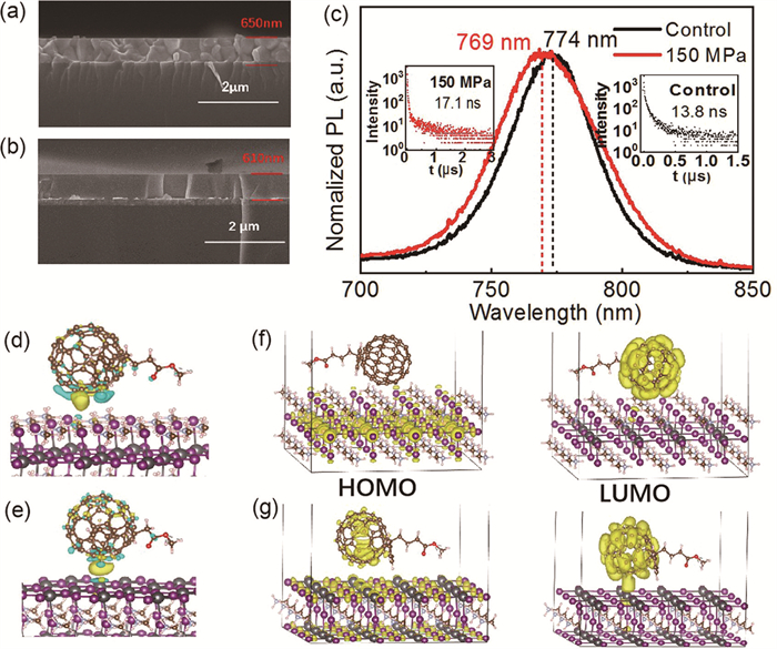
The detailed information of perovskite fabrication is shown in experimental section. Besides the normal preparation (Fig. 1a), further improvement in perovskite layer has been done (Fig. 1b). During formation of perovskite layer, 150 MPa is applied to modify both the surface and bulk crystallization. Crystallization becomes more better for the perovskite layer with high pressure treatment. The photoluminescence (PL) becomes more broadly, and PL peak shown blue-shift (Fig. 1c), which will prevent charge recombination effectively. Also, fluorescence lifetime is longer for the perovskite film with high pressure treatment, compared to the control samples. The perovskite with longer fluorescence lifetime will contribute to the electron-hole pairs dissociation to increase overall photo-current. Furthermore, for in-situ PL measurements, as shown in Fig. S1 (Supporting information), after finishing the perovskite PL measurement, solvent of dichlorobenzene (DCB) is dropped on perovskite surface. It is noted that PL does not change. Upon depositing the P3HT solution (using DCB as the solvent), the control perovskite’s PL exhibits quenching. For perovskites subjected to high-pressure treatment, the PL quenching is significantly more pronounced. Up to now, many studies have been done based on the improvement of the perovskite crystallization and interfacial engineering to enhance photovoltaics. Here, perovskite improvement dependence of both surface properties and interfacial spin effect on photovoltaics will be studied.
Figure 1
Figure 1.
SEM of perovskite layers of (a) control sample and (b) high-pressure treated sample. (c) PL quenching of perovskite layer after doping solvent. Charge density distribution of (d) PCBM/perovskite (100) crystal surface and (e) PCBM/ perovskite (110) crystal surface. HOMO and LUMO of (f) PCBM/perovskite (100) and (g) PCBM/perovskite (100).
Based on surface study, the roughness of the perovskite surface has not been significantly improved with applying external pressure treatment (Fig. S2 in Supporting information). In general, perovskite (110) and (100) crystal faces are more common for the surface to contact the transport layer. It is believed that perovskites with varying surfaces, when combined with organic layers to form transport layer/perovskite heterostructures, result in distinct interfacial charge distributions and charge dissociation efficiencies. As shown in Figs. 1d and e, charge density distributions are studied at heterostructure of PCBM/perovskite (100) and PCBM/perovskite (110) with identical distance between PCBM and perovskite layers, both of them present charge transfer between PCBM and perovskite crystal faces. However, the degrees of charge transfer are different. Differential charge values are 0.147e and 0.187e for PCBM/perovskite (100) and PCBM/perovskite (110), respectively. This result shows that optimizing the surface of perovskite and adjusting the surface crystal face will help improve the extraction of interfacial charges and increase photovoltaic efficiency. In the heterostructure composed of PCBM and perovskite (100), the highest occupied molecular orbital (HOMO) is localized within the perovskite, while the lowest unoccupied molecular orbital (LUMO) resides in the PCBM (Fig. 1f). In the heterostructure composed of PCBM and perovskite (110), the case is different. Although the LUMO is still located within the PCBM, the HOMO is presented in both the perovskite and the PCBM (Fig. 1g). This implies that electrons can be readily transferred from the perovskite to the PCBM, resulting in a more significant differential charge value. This is the reason why differential charge value is larger in the PCBM/perovskite (110) heterostructure than that in PCBM/perovskite (100) heterostructure.
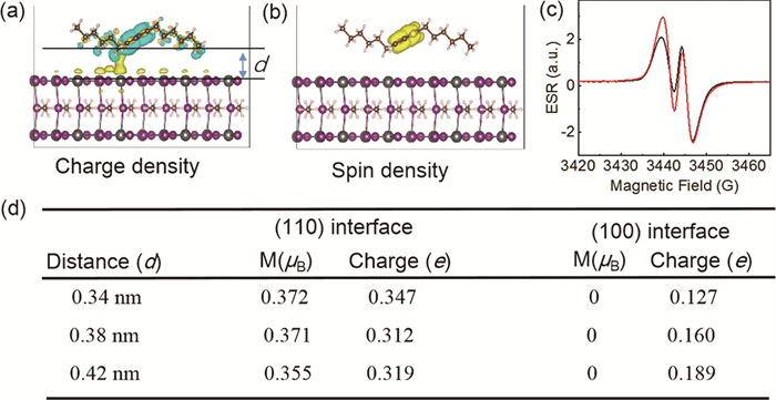
To further understand the key factors influencing the performance of interfacial charge transfer, the dependence of differential charge on interfacial spin polarization is studied. In the case of the PCBM/perovskite heterostructure, despite the presence of interfacial differential charges, no interfacial spin polarization has been detected. However, for P3HT/perovskite (110) heterostructure, the differential charge is significantly higher than that of PCBM-related heterostructures (Fig. 2). Also, both interfacial differential charge (Fig. 2a) and the interfacial spin polarization (Fig. 2b and Fig. S5 in Supporting information) can be clearly observed. The spin-polarized interface has the capability to generate a localized magnetic field. When exposed to this magnetic field, photoexcited electron-hole pairs undergo a transition from singlet to triplet states. Owing to the elevated dissociation rate of the triplet states, which is a consequence of the prohibition of spin transitions, interface polarization significantly enhances the extraction of charges at the interface. Because of the charge transfer that occurs at the interface between P3HT and perovskite, holes become localized within the P3HT, whereas electrons are dispersed throughout the perovskite. Given the distinct g-factors of electrons and holes, electron spin resonance reveals two distinct resonance signals (Fig. 2c). Besides P3HT/perovskite (110) heterostructure, P3HT/perovskite (100) heterostructure dependence of interfacial differential charge is also studied. The interesting thing is that P3HT/perovskite (100) interface cannot produce interfacial spin polarization (Fig. 2d and Fig. S6 in Supporting information), even with different interfacial configuration (Fig. S7 in Supporting information). As a result, the differential charge value is also very small in P3HT/perovskite (100) interface. Therefore, P3HT/perovskite (110) heterostructure with interfacial spin polarization is one of the key factors in enhancing the number of differential charges.
Figure 2
Figure 2.
(a) Differential charge density and (b) spin density distribution in P3HT/perovskite (110) heterostructure. (c) Electron spin resonance in P3HT/perovskite (110) heterostructure. (d) differential charge and interfacial magnetic moments in P3HT/perovskite (110) and P3HT/perovskite (100) heterostructures with different distance between P3HT and perovskite surface. The distance ranges from 0.34 nm to 0.42 nm.
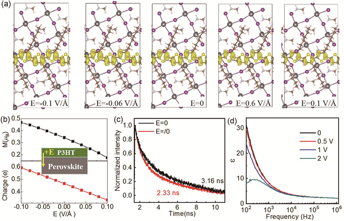
Though applying external electric field, interfacial differential charge and magnetic moment in P3HT/perovskite are further studied. As shown in Fig. 3a, when the electric field ranges from −0.1 V/Å to 0.1 V/Å, P3HT/perovskite interfacial spin density distribution present a pronounced change. The direction of applied electric field is shown in the inset of Fig. 3b. By applying a positive electric field, holes will not easily transfer from perovskite to P3HT, which will lead to a decrease in the interface differential charge (Fig. 3b and Table S2 in Supporting information) and interface spin polarization density (Figs. 3a and b) in P3HT/perovskite. On the contrary, if a negative external electric field is applied, holes will be more easily transferred from perovskite to P3HT, thereby increasing the interface differential charge and magnetic moment (Fig. 3b). Furthermore, the application of a positive external electric field can inhibit the transfer of holes from perovskite to P3HT, and also diminish the extent of the electric field within the interfacial region. Consequently, this facilitates the rapid recombination of electron-hole pairs, unimpeded by the electric field, thereby indicating that the fluorescence lifetime of perovskite is shortened in the presence of an external positive electric field (Fig. 3c). Applying a negative electric field will have the opposite effect. In addition, a shorter fluorescence lifetime due to a forward bias will reduce the concentration of electron-hole pairs, thereby reducing the dielectric constant (Fig. 3d). Thus, it should be noted that the differential charge density at the interface is closely related to the interfacial spin polarization, which will determine the charge extraction at the interface of the photovoltaic device. Enhancing the interface spin polarization will improve the interface charge transfer and charge extraction.
Figure 3
Figure 3.
(a) Spin density distribution in P3HT/perovskite (110) heterostructure with and without applying external electric field. Electric field ranges from −0.1 V/Å to 0.1 V/Å. (b) Electric field dependence of differential charge and magnetic moment in P3HT/perovskite (110) heterostructure. (c) Fluorescence lifetime of perovskite and (d) dielectric constant in P3HT/perovskite with and without applying external electric field.
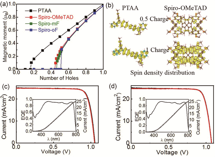
For the photovoltaic devices, besides P3HT, PTAA and Spiro-OMeTAD are used as charge transport materials to fabricate perovskite solar cells. PTAA and Spiro-OMeTAD present similar differential charge-interfacial spin polarization relationship. As shown in Fig. 4a, in the absence of interface spin polarization, the differential charge density is reduced. For instance, in the case of PTAA, without interface spin polarization, the interface differential charge density is small. However, the emergence of interface spin polarization significantly boosts the interface differential charge (Figs. 4a and b, Fig. S7 in Supporting information), playing a pivotal role in enhancing charge extraction in photovoltaic devices. A similar situation was also observed in Spiro-OMeTAD (Figs. 4a and b). Hence, it is reasonable to infer that the enhancement in charge extraction efficiency, resulting from interface spin polarization, will positively impact the efficiency of photovoltaic devices.
Figure 4
Figure 4.
(a) The relationship between extracted charge and spin polarization. (b) Spin density distribution of PTAA and Spiro-OMeTAD with different magnitudes of extracted charge. J-V curves of devices of (c) FTO/SnO2/PVK/PTAA/Au and (d) FTO/SnO2/PVK/Spiro-OMeTAD/Au. The insets of them present EQE studies.
The device structure featuring FTO/SnO2/PVK/transport layer/Au are design for PTAA, and Spiro-OMeTAD with PCE (power conversion efficiency) of (22.15±0.27)%, and (23.19±0.35)%, respectively (Figs. 4c and d). The VOC are nearly the same for these three devices, around 1.14 V. However, the photocurrents present a pronounced difference. With identical interfacial spin polarization, larger interfacial differential charge will be generated in Spiro-OMeTAD, compared to PTAA. As a result, for the device FTO/SnO2/PVK/Spiro-OMeTAD/Au, the JSC is 25.19±0.41 mA/cm2, which is much larger than that of FTO/SnO2/PVK/PTAA/Au, 24.34±0.30 mA/cm2. Thus, the enhanced charge extraction due to higher interfacial spin polarization can significantly increase the overall photocurrent, thereby achieving a high PCE.
In summary, with the high pressure treatment on perovskite layer, high pressure is applied to modify both the surface and bulk crystallization. the surface of the perovskite with and without high pressure present (110) and (100) dominated crystal faces. With different charge transport layer P3HT, PTAA, and Spiro-OMeTAD to connect perovskite forming heterostructures, interfacial spin polarization dependence charge extraction are studied. The spin density distributions can be only observed in perovskite crystal faces of (110) dependent heterostructures, where larger interfacial spin polarization will contribute to the interfacial charge extraction. Based on photovoltaic devices fabrication, it is obtained that the enhanced charge extraction due to higher interfacial spin polarization can significantly increase the overall photocurrent, thereby achieving a high power conversion efficiency.
Declaration of competing interest
The authors declare that they have no known competing financial interests or personal relationships that could have appeared to influence the work reported in this paper.
CRediT authorship contribution statement
Hua Peng: Investigation, Formal analysis, Data curation. Dong Hou: Investigation, Formal analysis. Jing-Hua Guo: Investigation, Data curation. Yuan Yu: Writing – original draft, Investigation, Data curation. Wei Qin: Writing – review & editing, Visualization, Supervision, Project administration, Investigation.
Acknowledgments
This work was supported by the National Natural Science Foundation of China (NSFC, Nos. T2222004, 92361301 and 62174102). Major Program of Shandong Province Natural Science Foundation (No. ZR2024ZD45).
Supplementary materials
Supplementary material associated with this article can be found, in the online version, at doi:10.1016/j.cclet.2025.111081.
Figure 1
SEM of perovskite layers of (a) control sample and (b) high-pressure treated sample. (c) PL quenching of perovskite layer after doping solvent. Charge density distribution of (d) PCBM/perovskite (100) crystal surface and (e) PCBM/ perovskite (110) crystal surface. HOMO and LUMO of (f) PCBM/perovskite (100) and (g) PCBM/perovskite (100).
Figure 2
(a) Differential charge density and (b) spin density distribution in P3HT/perovskite (110) heterostructure. (c) Electron spin resonance in P3HT/perovskite (110) heterostructure. (d) differential charge and interfacial magnetic moments in P3HT/perovskite (110) and P3HT/perovskite (100) heterostructures with different distance between P3HT and perovskite surface. The distance ranges from 0.34 nm to 0.42 nm.
Figure 3
(a) Spin density distribution in P3HT/perovskite (110) heterostructure with and without applying external electric field. Electric field ranges from −0.1 V/Å to 0.1 V/Å. (b) Electric field dependence of differential charge and magnetic moment in P3HT/perovskite (110) heterostructure. (c) Fluorescence lifetime of perovskite and (d) dielectric constant in P3HT/perovskite with and without applying external electric field.
Figure 4
(a) The relationship between extracted charge and spin polarization. (b) Spin density distribution of PTAA and Spiro-OMeTAD with different magnitudes of extracted charge. J-V curves of devices of (c) FTO/SnO2/PVK/PTAA/Au and (d) FTO/SnO2/PVK/Spiro-OMeTAD/Au. The insets of them present EQE studies.

 DownLoad:

 下载:
下载:


 下载:
下载:
