Citation:
Shujun Ning, Zhiyuan Wei, Zhening Chen, Tianmin Wu, Lu Zhang. Curvature and defect formation synergistically promote the photocatalysis of ZnO slabs[J]. Chinese Chemical Letters,
2025, 36(7): 111057.
doi:
10.1016/j.cclet.2025.111057
Curvature and defect formation synergistically promote the photocatalysis of ZnO slabs
English
Curvature and defect formation synergistically promote the photocatalysis of ZnO slabs
College of Chemistry, Fuzhou University, Fuzhou 350108, China
b.
State Key Laboratory of Structural Chemistry, Fujian Institute of Research on the Structure of Matter, Chinese Academy of Sciences, Fuzhou 350002, China
c.
Fujian College, University of Chinese Academy of Sciences, Fuzhou 350002, China
d.
University of Chinese Academy of Sciences, Beijing 100049, China
e.
Fujian Provincial Key Laboratory of Theoretical and Computational Chemistry, Xiamen 361005, China
f.
Key Laboratory of Opto-Electronic Science and Technology for Medicine of Ministry of Education, Fujian Provincial Key Laboratory of Photonics Technology, College of Photonic and Electronic Engineering, Fujian Normal University, Fuzhou 350117, China
* Corresponding authors. E-mail addresses: wtm@fjnu.edu.cn (T. Wu)
Received Date:
29 October 2024 Accepted Date:
07 March 2025 Revised Date:
17 February 2025 Available Online:
15 July 2025
Abstract:
Crystal defects and morphological modifications are popular strategies to enhance the catalytic activity of heterogeneous semiconductor photocatalysts. Despite defect engineering and morphology control show their successful applications in ZnO, the effects of curved surface modifications on the photocatalytic performance of ZnO and their interplay with the defect formation remain unclear. To resolve this puzzle, we systemically investigate the joint effects of curvature and defect formation on the electronic structure, optoelectronic properties, and photocatalytic performance of ZnO slabs using first-principles calculations. We find that curvature deformation effectively narrows the electronic bandgap by up to 1.6 eV and shifts the p-/d-band centers, thereby enhancing light absorption in the visible and near-ultraviolet regions. Besides, curvature deformation stimulates self-polarization, facilitating the separation of photo-generated electrons and holes. Also, curvature deformation promotes the formation of defects by reducing defect formation energy (by up to 1.0 eV), thus creating abundant reaction sites for photocatalysis. Intriguingly, the synergistic interaction between curvature and defect deformation further strengthens the self-polarization, narrows the electronic bandgaps, adjusts the p-/d-band centers to improve the optoelectronic properties, and influences the dissociation and free energy barriers of intermediates. Consequently, our findings reveal that this synergy substantially enhances the photocatalytic performance of ZnO slabs, providing deeper insights into the role of defect engineering and morphology control on photocatalysis.
Industrialization has significantly improved the convenience of human life, but it has also resulted in the emission of large amounts of greenhouse gases, contributing to climate change and causing severe damage to the global ecosystem [1-4]. Heterogeneous semiconductor photocatalysis has long been regarded as one of the most promising approaches to tackling the myriad environmental issues [5-9]. In light of this, ZnO photocatalysts stand out for their unique virtues, involving a large direct electronic bandgap (~3.37 eV), high carrier mobility, excellent chemical stability, and diverse nanostructures with abundant defect sites [10,11]. These features render ZnO an appealing candidate with extensive application prospects in photocatalysis and photoelectrocatalysis [11].
To date, numerous strategies have been developed to enhance the photocatalytic performance of ZnO. Among them, defect engineering and morphological modifications are commonly applied [12-14], including facet and size regulation, ligand modification, surface doping, dimensionality reduction, and interface engineering. Besides, integrating two strategies has shown great potential to further promote the catalytic activity of ZnO. For example, simultaneous optimization of morphology and vacancy defects has obviously improved the photocatalytic performance of ZnO in degrading gaseous formaldehyde [15]. Additionally, preparing ZnO slabs with a large specific surface area and high oxygen vacancy concentration has enabled efficient visible-light photocatalysis [16]. These advancements underscore the critical role of defect engineering and morphological modification in enhancing the performance of ZnO and suggest their synergistic effect.
Unlike traditional morphological modifications, which focus on controlling size, crystallographic orientation, and surface properties [17], recent advancements in curved surface structures have introduced novel morphologies for nanocatalysts, such as nanotubes [18], nanorods [19], and streamlined shapes [20]. This offers an alternative approach for designing nanocatalysts with efficient light absorption and well-matched energy band edges, facilitating carrier transport to reaction sites, inhibiting the recombination of photogenerated electrons and holes [17], and ultimately boosting photocatalytic activity [21]. Even so, current experimental approaches are insufficient to reveal the structure-property relationships and the underlying microscopic physical mechanism. Moreover, the combined effects of curvature and defects on photocatalytic efficiency are not well understood.
Herein, based on first-principles calculations (with more methodological details provided in Supporting information), we theoretically investigate the effects of curvature and defect formation on the electronic structure, optoelectronic properties, and photocatalytic performance of ZnO slabs. More importantly, we aim to reveal, from a theoretical perspective, the molecular mechanism underlying the combined effects of curvature and defects on the regulation of photocatalytic performance. Our findings are expected to provide deeper insights into the interplay between the curved surface structure and defect engineering, offering an alternative strategy to improve the catalytic activity of heterogeneous semiconductor photocatalysts.
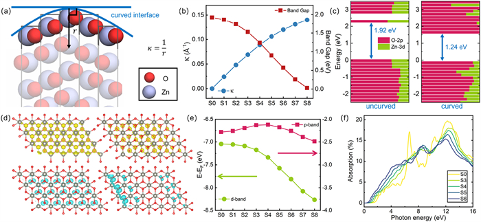
Due to the complexity of nanosheet morphological modification, constructing an effective model is a top priority for theoretically investigating the influence of curvature on photocatalysis and the intrinsic mechanisms. However, there is still no established rule for constructing such models. Inspired by the previous curved models constructed for two-dimensional materials [22-24], we propose to artificially stress the atoms exclusively in the z-direction, generating a periodic strain gradient to simulate the combined effects of curvature deformations and defects on the electronic structure and photocatalytic performance of ZnO slabs. Particularly, in comparison with the uncurved model named S0, a series of curved ZnO slabs named S1~S8 with the surface curvature κ equaling 0.024, 0.048, 0.069, 0.089, 0.106, 0.120, 0.131, and 0.140 Å-1 were constructed after imposing different z-directional displacements based on the configuration of uncurved ZnO (0001) surfaces (Figs. 1a and b, and Fig. S1a in Supporting information, see Supporting information Section 1 for details).
Figure 1
Figure 1.
(a) Schematic diagram of the curvature model for ZnO slab. (b) Curvature values (blue) and bandgaps (red) of the uncurved and eight curved ZnO structures. (c) Partial density of states (PDOS) for uncurved and curved (0.089 Å-1, S4) ZnO slabs. (d) The conduction band maximum (CBM, yellow) and valence band maximum (VBM, cyan) orbital arrangements of uncurved (left) and curved ZnO slabs (0.089 Å-1, S4, right). (e) The variation of the d-/p-band centers in ZnO as a function of curvature. (f) The light absorption coefficients of the curvature-dependent linear absorption spectrum of ZnO slabs.
To investigate the impact of curvature on photocatalysis, the electronic band structures and partial density of states (PDOS) for both curved and uncurved ZnO slabs were calculated. The orbital projected electronic band structure of the uncurved ZnO slab along high-symmetry points and the PDOS reveal that both the valence band maximum (VBM) and the conduction band maximum (CBM) are located at Γ high symmetry point dominated by the hybridization of O-2p and Zn-3d orbitals (Fig. 1c and Fig. S1b in Supporting information). Even so, the electronic bandgap decreases from 1.89 eV to 0.26 eV as the curvature increases from 0 Å-1 (S0) to 0.131 Å-1 (S7) (Fig. 1b and Fig. S1b in Supporting information). Interestingly, in addition to the electronic bandgap, the band structure undergoes notable changes with increasing curvature (Fig. S2a in Supporting information). Specifically, as curvature increases, the delocalized states move closer to the top of the valence band, while the localized states remain at the VBM at the Γ point. Additionally, the curvature modulation causes the valence band states at the C high-symmetry point to rise toward the Fermi energy level (EF), bringing them closer to the Γ high-symmetry point, potentially forming an indirect bandgap beyond the Γ point. Besides, the PDOS of ZnO slabs with varying curvature further reveals that the conduction band edge shifts toward the EF, narrowing the electronic bandgaps as curvature increases. However, the overall shape of the conduction band remains nearly unchanged.
In semiconductor photocatalysts, self-polarization contributes to the formation of a built-in electric field under photo-irradiation, accelerating the separation and migration of photo-generated holes and electrons to opposite surfaces. The VBM and CBM orbital arrangements, as shown in Fig. 1d and Fig. S2b (Supporting information), demonstrate that curvature deformation causes the electron wave functions of VBM and CBM to delocalize at the surface and leads to a shift from a regular and stable distribution to a relatively unstable and polarized state within the ZnO slabs. The observed self-polarization effect in curved ZnO slabs is expected to promote photocatalytic reactions by accelerating the separation and migration of electrons and holes toward opposite directions, facilitating their movement to the material surface after photoexcitation. Furthermore, the reduction in excitation energy resulting from the decreased electronic bandgap after curving is expected to further improve the photocatalytic performance of ZnO slabs.
Along with favorable electronic bandgaps, the d-band and p-band centers are crucial metrics in evaluating photocatalytic performance, thus serving as alternative targets for optimizing photo-electrocatalytic materials [25-27]. For ZnO, the d-band center plays a critical role in regulating two competing reactions [28,29]: A positive shift enhances the hydrogen evolution reaction (HER), whereas a negative shift favors the CO2 reduction reaction (CO2RR). In contrast, although the exact role of the p-band centers of O in ZnO catalytic reactions remain unclear, changes in the p-band centers have been observed to correlate with the catalytic effects [30,31]. To evaluate their variations with curvature, the d-band and p-band centers of both uncurved and curved ZnO slabs are calculated. As shown in Fig. 1e, curvature primarily affects the d-band centers rather than the p-band centers. With increasing curvature, the d-band centers shift significantly away from the EF, showing a 1.22 eV difference between S0 and S8. Meanwhile, the p-band centers exhibit a smaller variation, initially increasing by 0.16 eV from S0 to S4 and then decreasing by 0.20 eV at S8 compared to S0 as curvature increases. The decrease in the d-band centers with increasing curvature appears to enhance the reaction’s selectivity toward CO production [29], thereby promoting the CO2RR for CO production. Conversely, the slight rise in the p-band centers at lower curvatures may improve the chemisorption of intermediates, favoring efficient H2 generation [31] as well as ORR and OER reactions. As a result, the curved ZnO slab demonstrates significant potential as a photocatalyst in these reactions.
In addition to the curvature-dependent electronic bandgaps and d-/p-band centers of ZnO slabs, the optoelectronic properties are also crucial for photochemical reactions. Specifically, the curvature-dependent linear absorption coefficients and optical conductivity of ZnO slabs are evaluated to assess the capacity of semiconductor materials to absorb light across various wavelengths. As illustrated in Figs. S3a and b (Supporting information), the absorption spectrum reveals that ZnO slabs exhibit significantly enhanced band edge absorption and a pronounced blue shift compared to bulk ZnO, which is attributed to the widened electronic bandgap (Table S1 in Supporting information). This demonstrates the superior light absorption properties of the two-dimensional structure compared to the bulk one. As the curvature of the ZnO slab increases, the band edge absorption progressively redshifts, accompanied by an enhanced absorption observed in the visible and near-ultraviolet regions (Fig. 1f), suggesting that curvature deformation obviously enhances the optoelectronic properties of ZnO slabs. Such observations can be attributed to the narrowing electronic bandgap, as observed in Fig. 1b. Additionally, the curvature-dependent optical conductivity of ZnO slabs (Fig. S3c in Supporting information) shows that the real part of optical conductivity increases with increasing curvature, particularly in the visible and near-ultraviolet regions, aligning with the trend in the linear absorption coefficients (Fig. 1f).
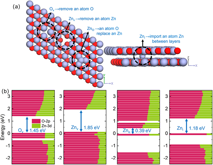
To investigate the impact of defect formation on the optoelectronic properties and photocatalytic performance of ZnO, we introduced various types of defects (Fig. 2a) at a moderate concentration, including oxygen vacancy (Ov), zinc vacancy (Znv), zinc anti-site (Zno), and zinc interstitial site (Zni), onto the uncurved ZnO surfaces. Subsequently, the defect formation energy (ΔEf) of each model is calculated to assess the ease of defect formation (see Supporting information Section 1 for details). As shown in Table S2 (Supporting information), the calculated ΔEf values of the uncurved ZnO slabs indicate that Ov and Zni defects are more likely to form under oxygen-poor conditions, while Znv defect is more favored under oxygen-rich conditions. The electronic band structure and PDOS for the uncurved ZnO slab with various defects (Ov, Znv, Zno, and Zni) reveal that impurity bands from Ov, Zno, and Zni defects appear within the bandgap (Fig. 2b). The emergence of impurity states results in a reduction of the electronic bandgap and the formation of new occupied states in the uncurved ZnO slab. In the case of Znv defects, the EF is situated within the valence band, imparting a certain degree of metallicity to the uncurved ZnO slab. These defect-induced modifications to the electronic band structure are consistent with previous studies [32,33], emphasizing that introducing defects on the surfaces of nanoparticles or nanosheets can effectively narrow the electronic bandgaps and alter the photocatalytic properties.
Figure 2
Figure 2.
(a) ZnO (0001) defect slab models featuring four types of defects. (b) PDOS of ZnO defect models.
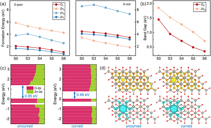
To further explore the combined effects of curvature and defect formation, we choose representative ZnO slabs S3-S6 (curvature of 0.069 Å-1, 0.089 Å-1, 0.106 Å-1, and 0.120 Å-1) with favorable direct electronic bandgaps, optimal band edge positions, modified d-/p-centers, and enhanced band edge absorption for the subsequent analysis. We first computed the ΔEf upon curvature and compared it to the uncurved ZnO (0001) slab. We find that the calculated ΔEf values of the curved S3-S6 models are generally lower than that of the uncurved S0 model, indicating that defect formation becomes easier upon curvature. Notably, the formation energy of Znv defect drops by approximately 1 eV as curvature increases from 0 Å-1 (S0) to 0.120 Å-1 (S6). Besides, ΔEf decreases gradually with increasing curvature under both O-rich and O-poor conditions (Fig. 3a), suggesting that the ease of defect formation is associated with the degree of curvature. Although curvature lowers the ΔEf, it barely changes the relative ease of forming various defects. Specifically, Ov and Zni defects are still more likely to form than Zno and Znv defects under oxygen-poor conditions, while Znv defect remains the most favorable defect under oxygen-rich conditions.
Figure 3
Figure 3.
(a) Relationship between defect formation energy (ΔEf) and curvature under O-poor and O-rich conditions. (b) The bandgap variation with curvature for the curved ZnO slab models with Ov and Znv defects. (c) PDOS of uncurved (left) and curved (0.089 Å-1, S4, right) ZnO slab models with Ov defects. (d) CBM (yellow) and VBM (cyan) orbital arrangements of uncurved ZnO and curved (0.089 Å-1, S4) ZnO slab models with Ov defects, respectively.
Besides the ΔEf, the electronic bandgap also decreases with increasing curvature of ZnO slab in the presence of Ov and Znv defects (Fig. 3b), consistent with the effect of curvature alone (Fig. 1b). The situation is more complex for the other two defects, but a general decreasing trend is observed (Fig. S4 in Supporting information). Different from the bandgap, the variations of the PDOS of the curved ZnO slabs are dependent on the defect type. In the presence of Ov defects (Fig. 3c), the curvature raises the valance band while narrowing the bandgap between the valence band and the impurity band (Fig. S5 in Supporting information). Simultaneously, the conduction band decreases and shifts closer to the EF. These curvature-induced modifications in both the valence and conduction bands reduce the electronic bandgap, facilitating the photoexcitation of electrons from the valence band through the impurity band into the conduction band, where they become free carriers. The VBM and CBM orbital arrangements of uncurved and curved ZnO with Ov defects (Fig. 3d and Fig. S5 in Supporting information) reveal that curvature amplifies the Ov-induces electron polarization, generating active sites favorable for reactions. For Zni defect in ZnO slab, the effect of increasing curvature on the electronic structure is similar to that of Ov defects, but the bandgap between the impurity band and valence band of Zni narrows gradually (Fig. S6 in Supporting information). After a certain curvature (0.120 Å-1, S6), the impurity band integrates into the valence band. Meanwhile, the electronic bandgap of ZnO slab with Zni defects also narrows as curvature increases, primarily due to a decrease in the conduction band, though this reduction is less pronounced than that observed with Ov defects. For Zno defects, two impurity bands emerge: one intersects the EF and gradually approaches the declining conduction band as curvature increases, while the other is situated above the valence band and shifts toward EF (Fig. S7 in Supporting information). After reaching a certain degree of curvature, the impurity band merges into the conduction band, causing EF to traverse the conduction band and impart some metallic characteristics to the ZnO slab. In the case of Znv defects, increasing curvature leads to a gradual decrease in the conduction band, whereas the position of the valence band relative to EF remains relatively stable (Fig. S8 in Supporting information). However, the EF also intersects the valence band, imparting certain metallic properties to the ZnO slab with Znv defects, while the bandgap still tends to decrease as curvature increases. The above comprehensive analysis of bandgap and PDOS of curved ZnO slabs with various types of defects together indicates that structural curvature amplifies the modifications to the electronic band structure achieved by various defects (e.g., Ov, Zni, Zno, and Znv).
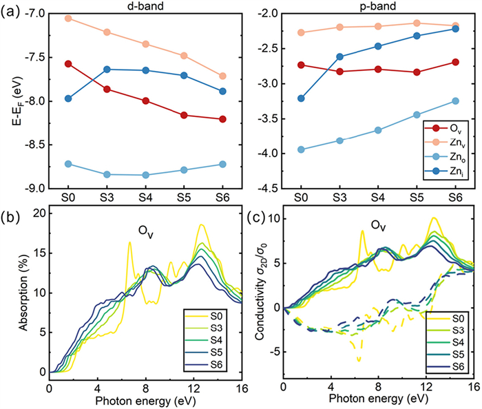
The combined effect of curvature and defect formation also markedly alters the d-/p-band centers. As shown in Fig. 4a, the curvature-induced modifications in the d-/p-band centers of the curved ZnO slabs with various types of defects are not entirely consistent with those without defects (Fig. 1e). In most cases, a decrease in the d-band centers and an increase in the p-band centers are observed, with the most significant changes occurring in the d-band centers for Ov defects (−0.63 eV) and Znv defects (−0.66 eV), as well as in the p-band centers for Zni defects (0.99 eV) and Zno defects (0.70 eV). This pattern, similar to the curved ZnO slab (Fig. 1e), indicates that curvature deformation can alter the d-/p-band centers and effectively influence photocatalytic reactions. In addition to the d-/p-band centers, the narrowing electronic bandgaps and enhanced band edge absorption clearly demonstrate an improved linear absorption coefficient in the visible and near-ultraviolet regions (Figs. 4b and c, Fig. S9 in Supporting information). Specifically, for the curved ZnO slab with various types of defect modifications, increasing curvature leads to an increment in the linear absorption (Fig. 4b and Fig. S9a), similar to that observed in the curved ZnO slab without defects (Fig. 1f). Consistently, Fig. 4c and Fig. S9b reveal a corresponding trend in the modifications of optical conductivity with increasing curvature. These alterations in the optoelectronic properties, stemming from the curvature-defect deformation, are expected to facilitate photocatalytic reactions.
Figure 4
Figure 4.
(a) Trend of changes in d-/p-band centers with curvature for ZnO with various defects. (b) Light absorption coefficients of curved ZnO models with Ov defects. (c) Optical conductivity of curved ZnO models with Ov defects.
The above results show that curvature deformation not only promotes defect formation but also works in conjunction with defects to effectively regulate the electronic structures and enhance visible-light adsorption. To further explore whether these influences exerted by curvature deformation are dependent on the specific defect concentrations and positions, calculations were performed for Ov, Zni, and Znv defects on the ZnO slabs with representative curvatures of 0.089 Å-1 (S4) and 0.120 Å-1 (S6) in comparison with the uncurved ZnO slab (S0). The simulation results, presented in Figs. S10-S16 (Supporting information), are discussed in detail in Supporting information Section 2. In this main text, only the most common Ov defect is selected for brief analysis and discussion. We find that the above-mentioned influence of curvature on the ΔEf, electronic properties, and optoelectronic properties of ZnO slabs can be consistently observed at different concentrations and different positions of Ov defects, lending credence to the assertion of curvature deformation as an effective strategy for improving the photocatalytic activity. Moreover, our results reveal that a higher concentration of Ov defects would help to amplify the influence, further reducing the ΔEf and electronic bandgap (Figs. S10 and S11).
To summarize, using first-principles calculations, we have systematically explored the synergistic effects of curvature deformation and defect formation on the electronic structure, optoelectronic properties, and photocatalytic performance of ZnO slabs. Our simulations demonstrate that curvature deformation can significantly alter the band edge position and narrow the electronic bandgap, making it a reliable approach for adjusting the appropriate band edge position and bandgap in catalytic reactions. Additionally, curvature deformation promotes defect formation and modifies the electronic structure of defects, facilitating control over catalyst morphology and defect manufacturing. The ease of defect formation on the curved ZnO surfaces leads to substantial modifications in the electronic structure and optoelectronic properties. The synergy between curvature deformation and point defects dramatically improves photocatalytic performance. Specifically, this combination promotes polarization in the ZnO slabs, thereby facilitating the separation of photo-generated electrons and holes to minimize recombination. Furthermore, the curvature-defect synergy narrows the electronic bandgaps, adjusts the p- and d-band centers, improves light absorption in the visible and near-ultraviolet regions, and influences the dissociation and free energy barrier of intermediates. Overall, our study offers molecular insight into the influence of curvature deformation and point defects on photocatalytic performance, helping to decipher the structure-property relationship and orientate the rational design of efficient semiconductor catalysts. Moreover, these fundamental physicochemical insights are expected to be applicable to other metal oxides in the field of photocatalysis, such as TiO2 and WO3.
Declaration of competing interest
The authors declare that they have no known competing financial interests or personal relationships that could have appeared to influence the work reported in this paper.
This work was supported by the National Key R&D Program of China (No. 2021YFA1502300), the National Natural Science Foundation of China (Nos. 22103012, 22173105), the Natural Science Foundation of Fujian Province (Nos. 2024J01456, 2024J01191), the Self-deployment Project Research Program of Haixi Institutes, Chinese Academy of Sciences (No. CXZX-2022-GH10), and the CAS Youth Interdisciplinary Team.
Supplementary materials
Supplementary material associated with this article can be found, in the online version, at doi:10.1016/j.cclet.2025.111057.
[1]
A. Hezam, Q.A. Drmosh, D. Ponnamma, et al., Chem. Rec. 22 (2022) e202100299.
[2]
Z. Li, B. Han, W. Bai, et al., Sep. Purif. Technol. 324 (2023) 124528.
[3]
Y. Zhu, H. Ji, T. Huang, Y. Sun, H. Pang, Adv. Sustainable Syst. 8 (2024) 2400225.
[4]
Y. Wang, X. Huang, H. Fu, J. Shang, J. Mater. Chem. A 10 (2022) 24362–24372. doi: 10.1039/d2ta07167c
[5]
N. Serpone, A.V. Emeline, J. Phys. Chem. Lett. 3 (2012) 673–677. doi: 10.1021/jz300071j
[6]
F. Sordello, P. Calza, C. Minero, S. Malato, M. Minella, Catalysts 12 (2022) 1572. doi: 10.3390/catal12121572
[7]
P. Dhiman, G. Rana, A. Kumar, et al., Environ. Chem. Lett. 20 (2022) 1047–1081. doi: 10.1007/s10311-021-01361-1
[8]
D. Hao, Y. Liu, S. Gao, et al., Mater. Today 46 (2021) 212–233.
[9]
D. Hao, C. Liu, X. Xu, et al., New J. Chem. 44 (2020) 20651–20658. doi: 10.1039/d0nj04068a
[10]
Z.L. Wang, Mater. Today 7 (2004) 26–33.
[11]
A.A. Ansari, R. Lv, S. Gai, et al., Coordin. Chem. Rev. 515 (2024) 215942.
[12]
H. Arandiyan, S.S. Mofarah, C.C. Sorrell, et al., Chem. Soc. Rev. 50 (2021) 10116–10211. doi: 10.1039/d0cs00639d
L. Schmidt-Mende, J.L. MacManus-Driscoll, Mater. Today 10 (2007) 40–48.
Figure 1
(a) Schematic diagram of the curvature model for ZnO slab. (b) Curvature values (blue) and bandgaps (red) of the uncurved and eight curved ZnO structures. (c) Partial density of states (PDOS) for uncurved and curved (0.089 Å-1, S4) ZnO slabs. (d) The conduction band maximum (CBM, yellow) and valence band maximum (VBM, cyan) orbital arrangements of uncurved (left) and curved ZnO slabs (0.089 Å-1, S4, right). (e) The variation of the d-/p-band centers in ZnO as a function of curvature. (f) The light absorption coefficients of the curvature-dependent linear absorption spectrum of ZnO slabs.
Figure 3
(a) Relationship between defect formation energy (ΔEf) and curvature under O-poor and O-rich conditions. (b) The bandgap variation with curvature for the curved ZnO slab models with Ov and Znv defects. (c) PDOS of uncurved (left) and curved (0.089 Å-1, S4, right) ZnO slab models with Ov defects. (d) CBM (yellow) and VBM (cyan) orbital arrangements of uncurved ZnO and curved (0.089 Å-1, S4) ZnO slab models with Ov defects, respectively.
Figure 4
(a) Trend of changes in d-/p-band centers with curvature for ZnO with various defects. (b) Light absorption coefficients of curved ZnO models with Ov defects. (c) Optical conductivity of curved ZnO models with Ov defects.

 DownLoad:

 下载:
下载:


 下载:
下载:
