College of Chemistry and Materials, Key Laboratory of Fluorine and Silicon for Energy Materials and Chemistry of Ministry of Education, Jiangxi Normal University, Nanchang 330022, China
b.
State Key Laboratory of Structural Chemistry, Fujian Institute of Research on the Structure of Matter, Chinese Academy of Sciences, Fuzhou 350002, China
c.
Department of Materials Science and Engineering, City University of Hong Kong, Hong Kong SAR 999077, China
Received Date:
24 September 2024 Accepted Date:
26 November 2024 Revised Date:
15 November 2024 Available Online:
15 March 2026
Abstract:
Lead-free perovskite has become a shining pearl in the field of direct X-ray detection due to its non-toxicity and excellent optoelectronic properties. However, the high limit of detection (LoD) of X-ray detectors due to high current noise caused by high operating voltages is a major challenge to overcome. Here, we utilized a zero-dimensional lead-free perovskite ferroelectric material (NMP)3Sb2Br9 (1, NMP = N-methylpyrrolidine) to achieve ultra-low LoD self-driven X-ray detection. The self-driven detection mode without external bias has been proven to be an effective means of reducing LoD due to its low current noise characteristics. Additionally, the zero-dimensional distinctive isolated framework results in a high resistivity of 1.39 × 10¹¹ Ω cm, which effectively reduces the current noise and suppresses ion migration. By further combining the ferroelectric-induced bulk photovoltaic effect, the 1-based detector achieves an ultra-low LoD X-ray detection of 84.1 nGyair/s under the self-driven mode, which represents a quite advanced level in the lead-free perovskite X-ray detection region. Our work successfully achieved ultra-low LoD self-driven X-ray detection by combining ferroelectricity with high resistance, providing a promising avenue for the development of low LoD X-ray detectors.
X-ray detectors are widely used in clinical medicine, safety inspections, food quality monitoring, and scientific research due to their superior penetration and safe and fast signal conversion capabilities [1-4]. These applications drive ongoing research on high-performance X-ray detection materials. Organic-inorganic hybrid perovskites (OIHPs) demonstrate significant promise for advancement in the realm of X-ray detection, attributable to their exceptional X-ray absorption capacity, superior carrier migration lifetime, and excellent photoelectric conversion capability [5-8]. For instance, the MAPbI3-based (MA = methylamine) detector exhibited a noteworthy sensitivity (S) of 2.2 × 10⁸ µC Gyair−1 cm−2 and an exceptionally low limit of detection (LoD) of 0.1 nGyair/s, which surpasses the performance of conventional X-ray detection semiconductors [9]. In addition, high-performance OIHPs X-ray detectors, such as MAPbBr3 [10], (BA)2PbI4 (BA = n-butylamine) [11], and (o-F-PEA)2PbI4 (o-F-PEA = 2-fluorophenethylamine) [12] have also been developed. However, despite the excellent performance of the aforementioned devices, they typically necessitate an external power source to drive the separation of photogenerated carriers, which can result in severe ion migration and a considerable loss of energy [13,14]. Self-driven X-ray detector is a novel candidate device that can operate independently and sustainably without external bias in X-ray irradiation [15,16]. Building typical built-in asymmetric components based on p-n junctions or Schottky barriers is a traditional solution for manufacturing self-driven detectors, but the development of these detectors is severely limited due to their complex manufacturing processes [17-19]. In addition, although the construction of polar hybrid perovskites for self-driven X-ray detection using chiral molecules represents an efficient methodology, the scarcity and elevated cost of their raw materials are daunting [20-22]. In this situation, there is an urgent need to explore new methodologies to attain self-driven X-ray detection.
Ferroelectric semiconductor materials have switchable spontaneous polarization (Ps) properties, and in their ferroelectric phase, they are often accompanied by fascinating ferroelectric photovoltaic effects (FPVE), which can create a built-in electric field to spontaneously separate photo-generated carriers without applying external bias. Therefore, an open circuit voltage that can serve as a self-driven detection driving force can be observed in the orientation of Ps [23-27]. For instance, studies have demonstrated that perovskite ferroelectrics, including (MAOPA)2CsPb2Br7 [28] (MAOPA = 3-methoxypropylamine), (IPA)2PbBr4 [29] (IPA = isopropylammonium) and (NPA)2(EA)2Pb3Br10 [15] (NPA = neopentylamine, EA = ethylamine), are capable of exhibiting highly effective self-driven X-ray detection functionality. Regretfully, despite the exceptional self-driven X-ray detection capabilities of these OIHPs ferroelectric materials, the toxicity of "lead" poses a considerable threat to human health. An effective strategy to address this issue is to replace lead with metallic antimony (Sb). For example, the developed two-dimensional Sb-based perovskite ferroelectric material (DFPD)4AgSbI8 (4,4-DFPD = 4,4-difluoropiperidinium) [30] has been proven to be an excellent X-ray detection material, but its LoD is still relatively high (360 nGyair/s, under 10 V bias) due to the influence of ion migration. Therefore, designing detectors that can suppress ion migration and achieve lower LoD remains a daunting subject. Recently, studies have shown that zero-dimensional (0D) OIHPs, due to their special "isolated" structure, have high electrical resistivity. They can effectively suppress ion migration, reduce dark current, and ultimately achieve low detection limit X-ray detection [31-34]. On this basis, we believe that the use of zero-dimensional lead-free OIHP ferroelectric materials for the development of self-powered X-ray detectors is a promising avenue of research.
In this work, a high-quality single crystal X-ray detector based on 0D lead-free OIHPs ferroelectric material (NMP)3Sb2Br9 (1, NMP = N-methylpyrrolidinium) was constructed. Furthermore, 1 shows significant FPVE, with a photovoltaic value of 0.57 V, which indicates that it can function as a driving force for the separation and transport of photo-generated carriers, ultimately enabling high-performance self-driven X-ray detection. It is worth noting that due to its high resistivity of 1.39 × 10¹¹ Ω cm, 1 can effectively suppress ion migration. Therefore, at a bias voltage of 0 V, the LoD of 1 is as low as 84.1 nGyair/s, which represents a quite advanced level in the domain of lead-free perovskite X-ray detection and is more than 60 times lower than the current dose rate (α-Se, 5500 nGyair/s) of conventional X-ray medical imaging. This work successfully achieved low LoD self-driven X-ray detection by combining ferroelectricity with high resistance, providing a promising avenue for the development of low LoD X-ray detectors.
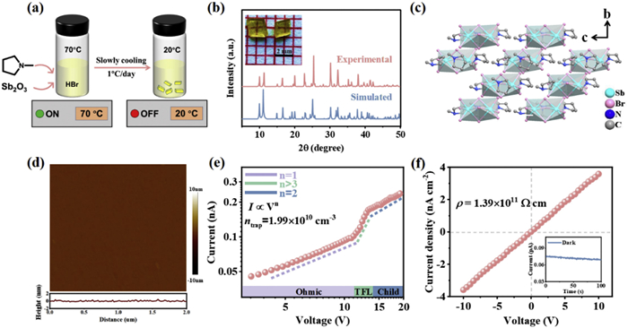
High-quality large crystals with a size of 2 × 2 × 1 mm3 were grown using a slow cooling method, the process schematic is shown in Fig. 1a, and the crystal morphology is illustrated in Fig. 1b (CCDC number: 1485752-1485753) [35,36]). Phase purity was confirmed using powder X-ray diffraction (PXRD) (Fig. 1b). The structural analysis shows that 1 belongs to a trigonal crystal system and that it crystalizes in the polar space group R3c at a temperature of 293 K. Its basic unit is made up of a discrete inorganic cluster [Sb2Br9]3− and three equivalent organic cations NMP+. Three of the nine bromine atoms in the inorganic cluster act as bridging linkers, coordinating with the central antimony atom of [Sb2Br9]3− (Fig. 1c). When the temperature rises to more than 322 K (Tc, phase transition temperature, as described below), both the inorganic and organic parts of 1 are strongly disordered. The inorganic skeleton of [Sb2Br9]3− employs a symmetrical configuration (space group: R3¯c), and all bridged bromine atoms are uniformly distributed between two equivalent octahedra (Fig. S1 in Supporting information). Then, the ferroelectric phase transition of 1 was validated using second harmonic generation (SHG), differential scanning calorimetry (DSC), and variable temperature dielectric constant measurements (Figs. S2–S5 in Supporting information). The thermogravimetric curve (Fig. S6 in Supporting information) showed that no significant weight loss was observed until 550 K, confirming the remarkable thermal stability of 1, which greatly favors its potential applications. The scanning electron microscopy (SEM, Fig. S7 in Supporting information) and the atomic force microscopy (AFM) images (Fig. 1d) show that the crystal surface is smooth without obvious defects [37,38]. Meanwhile, through analysis of the AFM data, the root mean square roughness (RMS) of the crystallographic plane is measured to be 0.383 nm, indicating the high quality of crystal 1. To further provide a detailed explanation of the quality of 1, the trap density (ntrap) was quantitatively measured using the Space Charge Limited Current (SCLC) method. As shown in Fig. 1e, the three different regions of the current-voltage (I–V) curve are the low voltage region (Ohmic, n = 1), the Trap-filled limited region (TFL, n > 3), and the high voltage region (Child, n = 2). The current increases gradually as the voltage increases in the low voltage region, and when the voltage reaches the TFL region, the current increases sharply. Its value can be calculated using the following formula [39,40]:
ntrap=2εε0VTFLeL2
(1)
Figure 1
Figure 1.
(a) Schematic for the growth of 1 crystals. (b) The experimental and simulated PXRD patterns of 1 (insert: crystal morphology of 1). (c) Structure of crystal 1 at a temperature of 293 K. (d) AFM images of the surface of 1. (e) I–V curve measurement by SCLC method. (f) The resistivity of Device 1, and the illustration show the dark current in self-driven mode.
Among them, L, e, ε and ε0 represent the interelectrode distance, the electron charge, the relative dielectric constant, and the absolute dielectric constant, respectively. Then, the ntrap value of 1 is 1.99 × 1010 cm−3, which is lower than several conventional inorganic semiconducting materials like Si (1013–1014 cm−3) [41], CdTe (1011–1013 cm−3) [42], and etc. Low crystal defect density exhibits a high crystal quality of 1, which facilitates the transport of photo-generated carriers for further development of high-quality optoelectronic detection devices. The high electrical resistivity of the material can effectively suppress ion migration, thereby reducing the LoD of the device. Therefore, the resistivity (ρ) of device 1 was measured (Fig. 1f). The calculated resistivity is as high as 1.39 × 10¹¹ Ω cm, which is analogous to the Cs2AgBiBr6 (1.6 × 10¹¹ Ω cm) [43] and (HIS)2AgSbBr8 (2.2 × 10¹¹ Ω cm) [44], much higher than that of MAPbX3 (X = Cl, Br, I; 107–108 Ω cm) [45-47]. Further compared with the same type of 0D materials, this value of 1 is also much higher than their values (Fig. S8 and Table S1 in Supporting information). As shown in the illustration in Fig. 1f, due to the high resistance of 1, its dark current is only about 0.07 pA. Such a low dark current will significantly reduce the LoD of the device, which is critical to efficient X-ray detection equipment.
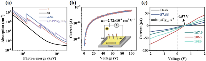
Optical and semiconductor properties are fundamental parameters that determine the range of material applications. The absorption cut-off edge of 1 is evaluated through ultraviolet-visible (UV–vis) absorption spectroscopy, with the result indicating that the absorption edges at 451 nm (Fig. S9a in Supporting information). Furthermore, the corresponding optical band gap of 1 is calculated to be 2.83 eV (insert image in Fig. S9a) in accordance with the Tauc equation. This value is close to the theoretically calculated value of 2.802 eV by the first-principles density functional theory (DFT) (Fig. S9b in Supporting information). Besides, the partial density of states (PDOS) clearly shows the attributions of different atoms in the band formation (Fig. S9c in Supporting information). It is obvious that the H-1s states overlap fully with C-2s and N-2s2p states in the range from −15 eV to 2.5 eV. In inorganic moieties, the conduction band minimum (CBM) arises from the Sb-5p orbitals while the valence band maximum (VBM) mainly stems from the Br-4p orbitals, thus the CBM and VBM of compound 1 are mainly contributed by the inorganic skeletons [35,36]. To realize direct X-ray detection, the material needs to absorb X-ray photons efficiently. Thus, the X-ray absorption capability of device 1 was calculated using a photon cross-section database. As shown in Fig. 2a, the results indicate that the absorptivity of 1 is much stronger than Si and is like the absorption coefficients of α-Se, CdTe, and (R-PPA)2BiI5 (R-PPA = R-1-phenylpropylamine) [20]. In addition, Fig. S10 (Supporting information) displays the thickness of these materials as a function of attenuation efficiency. Material 1 absorbs over 84% of the X-rays at a thickness of 1.0 mm and nearly all of them at a thickness of 3.0 mm, whereas crystalline Si absorbs only 23% of the X-rays. In addition, the charge collection efficiency of the device can be used to estimate the X-ray detection efficiency, which can be assessed by the mobility-lifetime (µτ) product. As shown in the insertion section of Fig. 2b, a single-crystal X-ray device was constructed along the polar axis (c-axis) of 1 (The photo of a single-crystal device of 1 as shown in Fig. S11 in Supporting information). Due to the powerful X-ray absorption capability of device 1, the µτ product can be obtained by fitting the modified Hecht equation [48]:
I=IoμτVL2[1−exp(−L2μτV)]
(2)
Figure 2
Figure 2.
(a) The absorption coefficients of 1 and other representative semiconductors versus photon energy. (b) Bias-dependent charge collection efficiency of 1 under X-ray illumination. Insert: Single crystal detector device diagram. (c) I–V curves under dark and X-ray irradiation.
Among them, I, I0, V, and L represent photocurrent, saturated photocurrent, bias voltage, and electrode spacing, respectively. The fitted µτ is 2.72 × 10⁻⁴ cm2/V under X-ray irradiation (Fig. 2b), which is greater than commercial α-Se thin films (about 10−7 cm2/V) [5], and similar with other lead-free OIHPs materials, such as (4,4-DFPD)4AgSbI8 (6.19 × 10⁻⁴ cm2/V) [30], Cs3Bi2Br9 (8.32 × 10⁻⁴ cm2/V) [32] and (S-PPA)4(PA)6Ag2Bi4I24 (2.44 × 10⁻⁴ cm2/V, S-PPA = S-1-phenylpropylamine, PA = propylamine) [49]. More importantly, as shown in Fig. 2c, the open-circuit voltage of 1 was found to be as high as 0.57 V under varying X-ray doses, which can be attributed to the ferroelectric built-in field of 1. This means that the photovoltage can be used as its power source, enabling effective X-ray detection.
To further demonstrate the FPVE of 1, a study was conducted with changes in the polarization electric field (Fig. 3a). The device was polarized before recording the current-voltage (I–V) curve, and then the I–V curve was recorded on 1 with X-ray irradiation. After positive/negative polarization, the open circuit voltage (Voc) and short circuit current (Isc) are −0.51 V/+ 3.6 pA and + 0.48 V/−3.1 pA, respectively. Therefore, the appearance of photocurrent in device 1 under zero applied electric field indicates that, like in other ferroelectrics, the charge carriers generated by light are separated and transmitted by the built-in electric field of the ferroelectrics [30,50,51]. Subsequently, the current density-time (J-t) curves of device 1 after positive/negative polarization under different X-ray irradiation doses were tested. As shown in Fig. 3b, perform positive polarization on device 1, and under sequentially increasing X-ray irradiation dose cycling on/off illumination, the direction of photocurrent remains unchanged. When a negative polarization is applied to device 1, the direction of the photocurrent also flips. This proves that the FPVE of 1 originates from its ferroelectricity and determines the direction of Isc. Meanwhile, it has also been determined that 1 can achieve self-driven X-ray detection.
Figure 3
Figure 3.
(a) I–V curves after positive-negative polarization. (b) Dependence of photocurrent direction on polarization direction. The upper and lower parts of the figure correspond to the direction of current after positive-negative polarization, respectively.
We have continued to investigate the X-ray response of the single crystal detector of 1. It is obvious from Fig. 4a that 1 shows excellent response to X-rays under 0 V bias. When the X-ray irradiation intensity increases from 4.35 µGyair/s to 44.77 µGyair/s, the photocurrent density of 1 rise from 1.13 nA/cm2 to 4.18 nA/cm2, and the device exhibited a perfect linear photocurrent response. The X-ray detection performance of the device was quantitatively evaluated by linear fitting of current density and X-ray dose rate, and a relatively high sensitivity (75.2 µC Gyair−1 cm−2) was achieved under zero bias voltage (Fig. 4b). Under self-driven mode, the sensitivity of 1 is higher than most lead-free OIHPs, such as (R-PPA)2BiI5 (31 µC Gyair−1 cm−2 under 0 V bias) [20], (BZA)2(R-PPA)BiI6 (53.2 µC Gyair−1 cm−2 under 0 V bias, BZA = benzylamine) [22] and (R-MPA)4AgBiI8 (46.3 µC Gyair−1 cm−2 under 0 V bias, R-MPA = R-β-methylphenethylammonium) (Table S2 in Supporting information) [21]. Excitingly, the remarkable sensitivity of 1 is much higher than that of classical inorganic materials, like α-Se (20 µC Gyair−1 cm−2 under 2000 V bias) and Si (8 µC Gyair−1 cm−2 under 0.5 V bias). As shown in Fig. 4c, device 1 also exhibited significant response at low doses of 1.089 µGyair/s and 2.234 µGyair/s, and its signal-to-noise ratios (SNR) were calculated to be 5.47 and 6.69, respectively. Besides, such a low signal-to-noise ratio means that 1 is a promising low LoD detection material, and its excellent performance at low doses also demonstrates its better safety and practical value in practical applications. In addition, as the X-ray irradiation intensity increases, device 1 still exhibits excellent response under different biases (Figs. S12–S14 in Supporting information). As the bias voltage is gradually increased to 50 V, the sensitivity of device 1 also increases accordingly (Fig. S15 in Supporting information). Furthermore, at a high bias voltage of 50 V, the sensitivity of 1 reaches its maximum value 1594.9 µC Gyair−1 cm−2 (Fig. S15) and is higher than many OIHPs, such as (PEA)4AgInBr8 [52] (185 µC Gyair−1 cm−2 under 200 V bias, PEA = phenethylammonium), (3AMPY)Pb2I6 [53] (207 µC Gyair−1 cm−2 under 200 V bias, 3AMPY = 3-(aminomethyl)pyridine) and (R-MPA)4AgBiI8 (949.6 µC Gyair−1 cm−2 under 50 V) (Table S1) [21]. At the same time, the excellent optical response exhibited by the device is more conducive to its practical application. The LoD is another important index to evaluate the performance of X-ray detection. The International Union of Pure and Applied Chemistry (IUPAC) has determined that the limit of detection is the X-ray dose rate corresponding to a signal-to-noise ratio of 3 [52]. The SNR value can be measured by the following equation:
SNR=Iphoto‾−Idark‾1N∑in(Ii−Iphoto‾)2
(3)
where the Iphoto‾ denotes the average photocurrent, Idark‾ denotes the average dark current, and Ii denotes the measured photocurrent. According to Fig. 4d, the LoD of 1 is calculated to be 84.1 nGyair/s in self-driven mode, which is much lower than many reported OIHPs, such as (R-PPA)2BiI5 [20] (2570 nGyair/s), (DFPD)4AgBiI8 (3130 nGyair/s) [54], (BDA)2PbI4 (430 nGyair/s) [8], (BA)2PbI4 (241 nGyair/s) [11], (S-BPEA)2FAPb2I7 (161 nGyair/s) (Table S2) [55]. More importantly, it has reduced the dose rate by more than 60 times compared to the current conventional X-ray clinical application (α-Se, 5500 nGyair/s) [13]. Furthermore, research was conducted on LoD under high external bias voltage. The data show that the LoD of the device under 10, 20, and 50 V bias are 274.5, 728.6, and 1731.2 nGyair/s, respectively (Figs. S16–S18 in Supporting information). The value of this degradation is due to the increase in dark current and noise caused by severe ion migration under high external bias voltage. In addition, the long-term operational and environmental stability of the device is critical in practical applications. The stability of the dark current is a key factor, and its stability can be evaluated in terms of the dark current drift (Idrift) with the following equation [56]:
Idrift=(It−Io)E×A×t
(4)
Figure 4
Figure 4.
(a) J-t curves of device 1 at 0 V bias. (b) Sensitivity values under different biases: obtained by fitting of the response current density and irradiance. (c) I–V curves and SNR of Device 1 at low doses of 1.089 µGyair/s and 2.234 µGyair/s, respectively. (d) The SNR dependent on X-ray intensity under 0 V bias. (e) The Idrift curves under 0 V and 50 V bias, respectively. (f) The stability of device 1 under continuous high-dose radiation. (g) Comparison of PXRD spectra between the fresh and three months later of 1. (h) Comparison of radiation response intensity and the fresh after being placed in the air for three months. (i) Comparison of sensitivity to the fresh and three months later at 0 V bias.
Among them, I0 and It are the initial and final dark currents, A is the area of the device, E is the test voltage, and t is the total test duration. It is thoroughly obvious that even with a high bias of 50 V, the device only produces a relatively small Idrift of 7.3 × 10⁻⁶ nA cm−1 s−1 V−1 (Fig. 4e). More importantly, this value is at least one order of magnitude lower than reported materials such as (BDA)(MA)2Pb3Br10 (3.18 × 10⁻⁴ nA cm−1 s−1 V−1, under 11.1 V/mm bias) [57], (R-PPA)2BiI5 (1.0 × 10⁻⁴ nA cm−1 s−1 V−1, under 10 V bias) [21], and (R-MPA)4AgBiI8 (1.02 × 10⁻³ nA cm−1 s−1 V−1, under 50 V bias) [21]. Then, the detector also received continuous X-ray irradiation at a dose operational stability under long-term irradiation (Fig. 4f). Remarkably, after receiving high-intensity irradiation with 2.59 Gyair, the device can still operate smoothly and continuously. Furthermore, the device can operate extremely stably in self-driven mode, highlighting its excellent radiation stability. Finally, the environmental stability of device 1 in the air was studied. As shown in Fig. 4g, after being exposed to air for three months, PXRD showed that the crystal of 1 had no significant phase change. Not only that, the sensitivity of device 1 was tested and compared after being exposed to air for three months. As shown in Fig. 4h and i, the signal intensity of the X-ray photoresponse of device 1 remains almost constant, and calculations show that the sensitivity of the device has been maintained at 93.6% (70.4 µC Gyair−1 cm−2) of its initial sensitivity. To further demonstrate its high stability, we tested the dark current drift of 1 after three months. As shown in Fig. S19 (Supporting information), the results show that its dark current drift value is as low as 8.7 × 10⁻⁶ nA cm−1 s−1 V−1, which is only a very slight change from the initial value (7.3 × 10⁻⁶ nA cm−1 s−1 V−1). In addition, as shown in Fig. S20 (Supporting information), device 1 still operates smoothly after being exposed to a high dose of X-ray irradiation of 167.9 µGyair/s for more than 600 s with a total dosage of 101.6 mGyair after three months. These results can fully confirm its excellent stability. Therefore, our work clearly demonstrates that the device we have developed is a high-performance and stable self-driven X-ray detection material.
In summary, we had successfully grown bulk crystals of 0D lead-free perovskite ferroelectric (NMP)3Sb2Br9 and further achieved high-performance self-driven X-ray detection. The X-ray detector based on 1 exhibits a significant FPVE, which utilizes this large photovoltage to drive the separation and transport of charge carriers, thus giving it the ability to self-driven X-ray detection. Meanwhile, 1 also has a high mobility-lifetime product of 2.72 × 10⁻⁴ cm2/V could allow for efficient charge collection. In the self-driven mode, 1 shows excellent X-ray response, showing a respectable sensitivity of 75.2 µC Gyair−1 cm−2 and an ultra-low LoD of 84.1 nGyair/s. And 1 also exhibits excellent long-term and high-dose irradiation operation stability and environmental stability. This exciting study offers a novel approach to the design of self-driven lead-free X-ray detectors in hybrid perovskites.
Declaration of competing interest
The authors declare that they have no known competing financial interests or personal relationships that could have appeared to influence the work reported in this paper.
CRediT authorship contribution statement
Huawei Yang: Writing – original draft, Software, Methodology, Formal analysis, Data curation. Jianbo Wu: Formal analysis, Data curation. Zeng-Kui Zhu: Writing – review & editing, Visualization, Supervision, Methodology, Investigation, Funding acquisition, Conceptualization. Hang Li: Software, Formal analysis. Panpan Yu: Software, Data curation. Ying Zeng: Formal analysis, Data curation. Qingran Ding: Software, Methodology, Data curation. Guirong Chen: Visualization, Software, Data curation. Lijun Xu: Software, Data curation. Zhangtong Han: Software, Formal analysis, Data curation. Haiqing Zhong: Formal analysis, Data curation. Yueying Wang: Software, Formal analysis. Wenhui Wu: Software. Junhua Luo: Writing – review & editing, Visualization, Supervision, Resources, Project administration, Methodology, Funding acquisition.
Acknowledgments
This work was financially supported by the National Natural Science Foundation of China (Nos. 22435005, 22193042, 22201284, 22305105, 22405108, 22175177, 22125110, 22122507, and U21A2069), the Key Research Program of Frontier Sciences of the Chinese Academy of Sciences (No. ZDBS-LY-SLH024), the Natural Science Foundation of Fujian Province (No. 2023J05076), the National Key Research and Development Program of China (No. 2019YFA0210402). the Natural Science Foundation of Jiangxi Province (Nos. 20224BAB213003, 20232BAB213020), Jiangxi Provincial Education Department Science and Technology Research Foundation (No. GJJ2200384).
Supplementary materials
Supplementary material associated with this article can be found, in the online version, at doi:10.1016/j.cclet.2024.110682.
W. Liu, T. Shi, J. Zhu, et al., Adv. Sci. 10 (2023) 2204512. doi: 10.1002/advs.202204512
[57]
S. Wang, F. Wang, X. Xu, et al., ACS Appl. Mater. Interfaces 15 (2023) 58566–58572. doi: 10.1021/acsami.3c12866
Figure 1
(a) Schematic for the growth of 1 crystals. (b) The experimental and simulated PXRD patterns of 1 (insert: crystal morphology of 1). (c) Structure of crystal 1 at a temperature of 293 K. (d) AFM images of the surface of 1. (e) I–V curve measurement by SCLC method. (f) The resistivity of Device 1, and the illustration show the dark current in self-driven mode.
Figure 2
(a) The absorption coefficients of 1 and other representative semiconductors versus photon energy. (b) Bias-dependent charge collection efficiency of 1 under X-ray illumination. Insert: Single crystal detector device diagram. (c) I–V curves under dark and X-ray irradiation.
Figure 3
(a) I–V curves after positive-negative polarization. (b) Dependence of photocurrent direction on polarization direction. The upper and lower parts of the figure correspond to the direction of current after positive-negative polarization, respectively.
Figure 4
(a) J-t curves of device 1 at 0 V bias. (b) Sensitivity values under different biases: obtained by fitting of the response current density and irradiance. (c) I–V curves and SNR of Device 1 at low doses of 1.089 µGyair/s and 2.234 µGyair/s, respectively. (d) The SNR dependent on X-ray intensity under 0 V bias. (e) The Idrift curves under 0 V and 50 V bias, respectively. (f) The stability of device 1 under continuous high-dose radiation. (g) Comparison of PXRD spectra between the fresh and three months later of 1. (h) Comparison of radiation response intensity and the fresh after being placed in the air for three months. (i) Comparison of sensitivity to the fresh and three months later at 0 V bias.

 DownLoad:


 下载:
下载:


