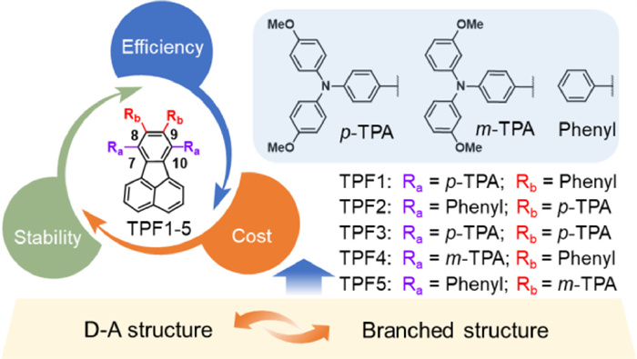
Figure 1.
Illustration of the design of dopant-free HTMs (TPF1–5).
Low-cost dopant-free fluoranthene-based branched hole transporting materials for efficient and stable n-i-p perovskite solar cells
Xinyu Yu , Fei Wu , Xianglang Sun , Linna Zhu , Baoyu Xia , Zhong'an Li

As a new generation of thin-film photovoltaic technology, perovskite solar cells (PVSCs) have made an incredibly rapid progress in power conversion efficiency (PCE) in a short period of time [1,2], thereby showing great potential for commercialization, combined with their advantages of low material cost of perovskites, compatible solution processing and high defect tolerance [3,4]. Currently, the long-term stability is the major obstacle to this commercialization progress [5–7], and one of the major reasons is the use of ionic and hydroscopic dopants in the processing of organic hole transporting materials (HTMs) [8–10]. Due to the typical sandwich device architecture of PVSCs, the HTMs play the critical roles in extracting and transporting holes, thus mitigating non-radiative recombination losses to ensure high device performance [11,12]. So far, most of the commonly used HTMs, such as 2,2′,7,7′-tetrakis(N,N-di-p-methoxyphenylamine)-9,9′-spirobifuorene (spiro-OMeTAD), unfortunately have low hole mobilities and conductivities, thus requiring an additional doping process with lithium bis(trifluoromethyl sulfonyl)imide (Li-TFSI) and 4-tert-butylpyridine (tBP) [13–15]. However, Li-TFSI is a hydroscopic salt that tends to undergo ionic migration, while tBP is volatile and can dissolve the perovskite, all of which are detrimental to the device stability of PVSCs [16–18].
The construction of dopant-free HTMs has been confirmed as an effective solution to overcome the instability caused by doping, and a variety of new dopant-free HTMs with PCEs over 22% have been developed [19–22]. The donor-acceptor (D-A) structure is a mainstream design strategy for dopant-free HTMs, as it can generate efficient intermolecular interactions to enhance hole mobility [23–25]. However, strong planar π-π stacking and intermolecular D-A interactions could affect the processability of HTMs and induce poor film morphology, which is detrimental to the contact of HTM with the perovskite and other layers [26]. Considering this problem, branched structure with high steric hindrance at the periphery has been reported to improve the film forming ability and thermal stability of the film morphology [27,28]. In this context, it is worthwhile to develop the D-A type branched HTMs, which is hopeful to simultaneously achieve efficient hole transport, good processability and stable film morphology.
Fluoranthene exhibits a rigid planar fused ring structure with an electron deficient character, which is favorable for improving thermal stability and π-π stacking [29,30]. In addition, it also has the advantages of easy synthesis and multiple functionalization sites. Our previous work has shown that fluoranthene is a suitable core unit for the construction of dopant-free D-A type HTMs, with PCEs above 20% realized [31,32]. Here, as shown in Fig. 1, we have further developed a class of fluoranthene-based D-A type branched HTMs (TPF1–5) with low lab synthetic costs by attaching different types of donor units such as para-methoxy substituted triphenylamine (p-TPA), meta-methoxy substituted triphenylamine (m-TPA) and phenyl unit to the fluoranthene core at different substitution sites (7,8,9,10-sites). The effect of structural variations on the HTM performance was elucidated, and among these new HTMs, the fabricated champion conventional PVSC based on TPF1 delivered the best PCE of 21.76%, which is comparable to the doped spiro-OMeTAD. What is more, benefiting from the removal of the dopants and the hydrophobic effect of HTM, the TPF1-based device showed a much better operational stability than the doped spiro-OMeTAD control device, which maintained over 87% of its initial PCE after 1038 h.
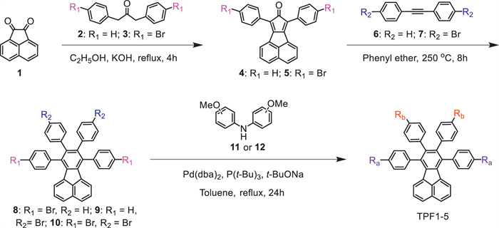
The synthetic route of TPF1–5 is shown in Scheme 1, with the synthetic details and characterization data provided in Supporting information. First, acenaphthenequinone (1) was reacted with dibenzyl ketone (2) or its brominated derivative (3) via the Knoevenagel reaction to afford compounds 4 and 5, respectively. They then underwent a typical Diels-Alder reaction followed by simple decarbonylation with diphenylacetylene (6) or its brominated derivative (7) to obtain the critical intermediates (8–10) with different degrees of bromination for further functionalization. Finally, TPF1–5 were synthesized by a Pd-catalyzed Buchwald-Hartwig reaction with satisfied yields between compounds (8-10) and bis(4-methoxyphenyl)amine (11) and bis(3-methoxyphenyl)amine (12), respectively. Overall, the entire synthesis process of TPF1–5 is simple and efficient due to the use of fluoranthene as the core, which therefore significantly reduces their synthetic costs. As shown in Table 1, the estimated lab synthesis costs of TPF1–5 are no more than 17 $/g, and the cheapest TPF2 has a cost of only 8.23 $/g, which is even less than one tenth of the lab synthesis cost of spiro-OMeTAD (91.67 $/g) [33].
 DownLoad:
CSV
DownLoad:
CSV

|
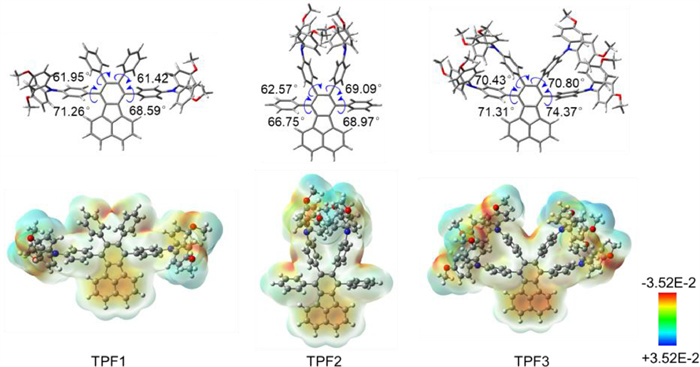
To understand the geometry structure and electron distribution, density functional theory (DFT) calculations were used to simulate TPF1–5 at B3LYP/6–31G(d, p) level with Grimme's D3BJ empirical dispersion correction (Fig. 2, Figs. S1 and S2 in Supporting information). As expected, all the peripheral arms attached to the planar fluoranthene are twisted with a torsion angle over 60°, and for TPF3, the four arms are even more twisted due to the large steric hindrance between the p-TPA units. The twisted arms may help to regulate the molecular stacking and improve the solution processability. In addition, the highest occupied molecular orbital (HOMO) and lowest occupied molecular orbital (LUMO) energy levels were also calculated, which are mainly located on the TPA units and the fluoranthene core, respectively. The HOMOs and LUMOs of TPF1–3 (–4.54/–1.66 eV, –4.53/–1.66 eV and –4.41/–1.55 eV, respectively) are higher than those of TPF4 and TPF5 (–4.83/–1.70 eV and –4.73/–1.66 eV, respectively), indicating that the substitution sites of fluoranthene core have a negligible effect on the energy levels, while the methoxy substitution sites show a pronounced effect owing to the inductive effect [34,35]. The slightly increased energy levels of TPF3 may be due to its more TPA substitutions. From the electrostatic potential (ESP) analysis, the fluoranthene core has a negative electrostatic potential with more electron cloud, confirming the push-pull electron effects in the D-A structure.
The optical, electrochemical, and thermal properties of TPF1–5 were characterized, with the data listed in Table 1. The UV–vis absorption spectra in dichloromethane (DCM) solutions and films are displayed in Figs. 3a and b, showing two absorption bands at around 300 and 400 nm, ascribed to the localized π-π* and intramolecular charge transfer (ICT) absorption, respectively. It is worth noting that TPF2 and TPF5 (TPA arms at 8,9-sites) exhibit an obvious and redshifted shoulder peak at ~380 nm compared to TPF1 and TPF4 (TPA arms at 7,10-sites) due to the different push-pull effects. The optical energy band gaps (Egs) are calculated by the film absorption edges, showing that TPF1–3 with p-TPA arms exhibit narrower Egs than TPF4–5 with m-TPA arms, and TPF3 has the narrowest Eg of 2.67 eV. This is because that the para-methoxy substitution can facilitate effective ICT, and TPF3 has more p-TPA substitutions.
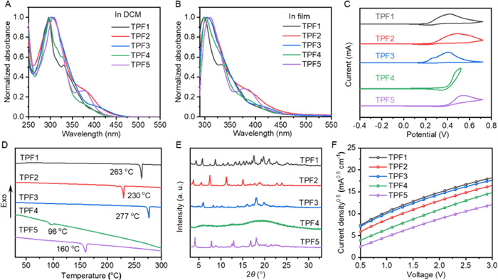
The electrochemical cyclic voltammetry (CV) curves of TPF1–5 films are presented in Fig. 3c, and the HOMO levels versus Fc/Fc+ were calculated to be about –5.0 eV for TPF1–3 and –5.2 eV for TPF4–5, respectively. The trend obtained from the CV results is consistent with that from calculation. It was further confirmed by the ultraviolet photoelectron spectroscopy (UPS) measurement (Fig. S3 in Supporting information), demonstrating that the HOMO levels of TPF1 and TPF4 are –5.24 and –5.39 eV, respectively. As reported [36–38], the differences in HOMOs between CV and UPS (~0.2 eV) may be due to the polarization/solvation energies or contact with the metal electrode in CV measurements. We further used the HOMO levels from the CV results to evaluate the LUMO levels by using the equation ELUMO = EHOMO + Eg, all of which were calculated to be about –2.3 eV.
Thermogravimetric analysis (TGA) and differential scanning calorimetry (DSC) measurements were performed under nitrogen at a heating rate of 10 ℃/min. From TGA curves in Fig. S4 (Supporting information), all HTMs show high thermal stability with similar onset temperatures of decomposition (Tds, corresponding to 5% weight loss) over 430 ℃, possibly due to the thermally stable fluoranthene core, which meets the requirement for an ideal dopant-free HTM [39,40]. In addition, TPF1–5 undergo different phase transitions according to the DSC analysis (Fig. 3d). TPF1–3 with p-TPA arms powders show a sharp peak with the melting points (Tms) of 263, 230, and 277 ℃, respectively, while TPF4 undergoes a phase transition at ~95 ℃ and TPF5 has a low Tm of 160 ℃. For TPF4 and TPF5, the meta-methoxy substitutions could break the symmetry of the molecular configuration and suppress the intermolecular interactions, making it difficult to detect Tm of TPF4 and lowering the Tm of TPF5 [41,42]. For TPF1–3, no phase transition can be found before melting over 230 ℃, which may help to maintain the stable film morphology during long-term operation of PVSCs [43,44].
On the other hand, the DSC results indirectly indicate that TPF1–5 have different molecular stacking behavior in the solid state [45]. To confirm this, we have collected the X-ray diffraction (XRD) patterns of their crystalline powders. As illustrated in Fig. 3e, TPF1 with p-TPA arms at 7,10-sites displays the most diffraction peaks with the strongest π-π molecular stacking diffraction peak, while TPF4 with m-TPA arms at 7,10-sites is difficult to observe any long-range ordered molecular stacking, indicating its amorphous state. These results thus suggest that the intermolecular interactions are influenced by both the number and position of substitutions on the fluoranthene core and the methoxy substitution sites, and either more branched structure or meta-methoxy substitution could suppress the intermolecular interactions.
As mentioned above, the hole mobility (μh) of HTMs is determined by the intermolecular interactions in the solid state, which needs to be high enough to be dopant-free. Therefore, we evaluated the μhs of dopant-free TPF1–5 films using the space charge limited current (SCLC) method with hole-only devices (ITO/PEDOT: PSS/HTM/MoO3/Ag). The corresponding J-V curves are shown in Fig. 3f and the fitted μhs of the HTMs are listed in Table 1. The μhs follow an order of TPF1 > TPF3 > TPF2 > TPF4 > TPF5, with the values of 8.23 × 10⁻⁵, 7.67 × 10⁻⁵, 5.13 × 10⁻⁵, 2.69 × 10⁻⁵, and 1.32 × 10⁻⁵ cm2 V−1 s−1, respectively, which are quite consistent with the XRD results. Compared to TPF4–5 with m-TPA arms, TPF1–3 with p-TPA arms show improved crystallinity and favorable film formation process to achieve higher μhs, possibly due to the less symmetrical structure of the former. Furthermore, the molecular structure of the TPA arms at 7,10-sites could be responsible for the highest μh of TPF1, allowing less steric hindrance to ensure much stronger π-π stacking, as evidence by XRD results.
The intermolecular interactions also affect the film morphology, which is important for the contact resistance of HTMs with other layers [46,47]. The atomic force microscopy (AFM) images of TPF1–5 films in Fig. S5 (Supporting information) show that TPF1, TPF3 and TPF5 exhibit more uniform and smoother film surface than TPF2 and TPF4 with a root mean square (RMS) surface roughness of less than 0.3 nm. Furthermore, the densely packed tiny grains can be observed in the images of TPF1 and TPF3, which however are invisible for TPF5, which indicates a relatively enhanced aggregation for TPF1 and TPF3 films, and thus well explains their high μhs. We also collected the AFM images of HTMs coated on the perovskite layer. As displayed in Fig. S6 (Supporting information), after covering with HTMs, the RMS of the perovskite layer decreased significantly from 24.6 nm to less than 17 nm, indicating that the HTMs can be uniformly coated and form better contact with other layers, which is further confirmed by their scanning electron microscope (SEM) images (Fig. S7 in Supporting information).
To investigate the device performance of TPF1–5, we fabricated conventional n-i-p PVSCs with an architecture of FTO/SnO2/Perovskite/HTM/MoO3/Ag (Fig. 4a), in which FA0.71MA0.29PbI2.71Br0.11Cl0.18 (FA: formamidinium, MA: methylammonium) was chosen as the photoactive layer and processed by a two-step method. The HTMs were processed by spin-coating method without dopants and the film thickness was controlled at 20–30 nm. Other device fabrication details are given in Supporting information. Fig. 4b shows the energy level alignment of the components in PVSCs, demonstrating that the HOMO levels of TPF1–5 are matched with the perovskites to extract the holes and the relatively high LUMO levels can efficiently block the electron transport [48].
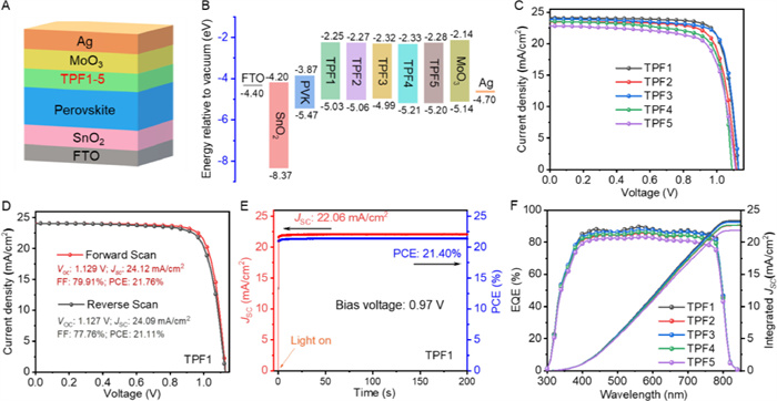
The current density-voltage (J-V) curves of champion PVSCs measured under AM 1.5 G irradiation at 100 mW/cm2 are shown in Fig. 4c, and the photovoltaic parameters are listed in Table 2. The device based on dopant-free TPF1 delivered the highest PCE of 21.76%, with an open circuit voltage (VOC) of 1.129 V, a short circuit current density (JSC) of 24.12 mA/cm2, and a fill factor (FF) of 79.91%. The PCEs of the champion devices based on TPF2–5 were 20.33%, 21.47%, 19.48%, and 18.73%, respectively. In addition, as shown in Fig. 4d and Fig. S8 (Supporting information), the forward and reverse scans of TPF1- and TPF3-based devices show negligible hysteresis with a calculated hysteresis index (HI) of only ~3% according to the equation of HI = (PCEforward-PCEreverse)/PCEforward, while other devices exhibit relatively high HIs exceeding 5%. It is impressive that dopant-free TPF1-based devices perform comparably to the doped Spiro-OMeTAD control devices (PCE = 22.21%, HI = 4.59%). The dopant-free devices were further operated at a constant bias near the maximum power point (MPP) for 200 s (Fig. 4e and Fig. S9 in Supporting information), and the TPF1-based device showed a stabilized PCE (21.40%) and a stabilized JSC (22.06 mA/cm2). Besides, the external quantum efficiency (EQE) spectra (Fig. 4f) of the TPF1–5 based devices were collected and the integrated JSC values were calculated to be 23.37, 22.64, 23.18, 22.70, and 21.88 mA/cm2, respectively, which are in good agreement with the actual experimental data. These results therefore confirm the reliability of the device performance. In addition, the histograms of the photovoltaic parameters are shown in Fig. S10 (Supporting information), suggesting good reproducibility for all dopant-free devices.
DownLoad:
CSV

|
Based on the device results, it is interesting to note that the device performance is highly correlated with the hole transport properties of the HTMs rather than the HOMO levels. As shown in Fig. S3, although TPF4 has a ~0.2 eV lower HOMO energy level than TPF1, they show an almost identical Fermi energy level, which could therefore allow a similar quasi-Fermi level splitting (QFLS) in devices. As reported, the QFLS dominates the VOC in PVSCs [49,50]. Furthermore, it is worth noting that in addition to the appropriate energy level alignment between HTM and perovskite, the non-radiative recombination loss at the interface also plays an important role in determining the VOC. Here, the smoother film morphology and higher hole mobility of TPF1 than TPF3 should help to reduce the contact resistance and facilitate the hole transport, thereby reducing the non-radiative recombination loss at the interface [51]. All the above factors finally lead to similar VOCs.
To futher deeply investigate the mechanism behind the device performance difference, the interfacial charge dynamics have been investigated by conducting steady-state photoluminescence (PL) and time-resolved PL decay measurements of pure perovskite films and those covered with HTMs, and the correpsonding sprctra are shown in Figs. 5a and b, with the detailed parameters listed in Table S2 (Supporting information). TPF1 and TPF3 can quench the PL to less than 10% of its initial intensity, with TPF1 performing better. The TRPL decay profiles are fitted by a biexponential decay function (I(t) = A1 exp(−t/τ1) + A2 exp(−t/τ2) + A0), where the decay profiles are separated into two exponential decay components, and the A1 and A2 are the weights of these two components in the overall decay process. The fast decay (τ1 < 30 ns) is attributed to the trap-mediated non-radiative recombination, while the slow decay (τ2 > 50 ns) is attributed to the radiative recombination [52,53]. Both τ1 and τ2 of the perovskite films are impressively reduced after covered with HTMs, with the average lifetime τave decreasing from 183.3 ns to less than 60 ns, with a trend of TPF1 < TPF3 < TPF2 < TPF4 < TPF5. These PL results therefore are consistent with their hole mobilities.
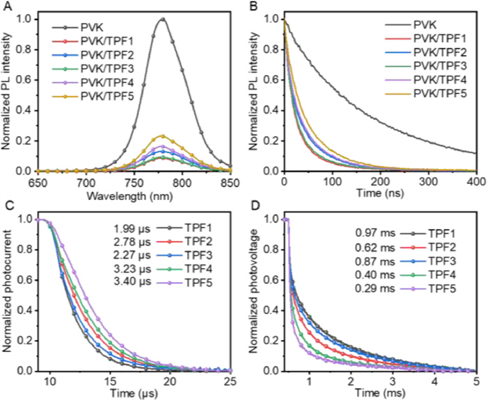
What is more, the calculated A1/A2 ratios show a significant difference, with a trend of PVK/TPF1 (217.0%) > PVK/TPF3 (203.8%) > PVK/TPF2 (87.4%) > PVK/TPF4 (67.1%) > PVK/TPF5 (54.1%) > PVK (4.3%). For conventional PVSCs, the bulk perovskite properties should have less influence on the A1/A2 ratios, so the difference in A1/A2 ratios could be attributed to the different interface induced by different HTMs [54,55]. These results further confirm that TPF1 and TPF3 exhibit a more efficient hole extraction than others. In addition, the good film contact of TPF1 and TPF3 can mitigate the defect density at the interface, well explaining their higher τ1 values [56,57].
We further measured the transient photocurrent (TPC) and transient photovoltage (TPV) decay curves to study the interfacial charge dynamics. The TPC curves in Fig. 5c show that TPF1–5 have the decay times of 1.99, 2.78, 2.27, 3.23, and 3.40 µs, respectively. The faster decay of the photocurrents in TPF1 and TPF3 also confirms their more efficient hole extraction and transport [58,59]. The decay time in TPV curve is usually attributed to the charge recombination. As shown in Fig. 5d, TPF1–5 exhibit the decay times of 0.97, 0.62, 0.87, 0.40, and 0.29 ms, respectively. The longer decay times of TPF1 and TPF3 can be due to the better contact with perovskite layer, which can reduce the recombination centers. Besides, the efficient hole extraction may also play a role in mitigating the recombination by reducing the density of the carriers [60,61], well corresponding to their TRPL results.
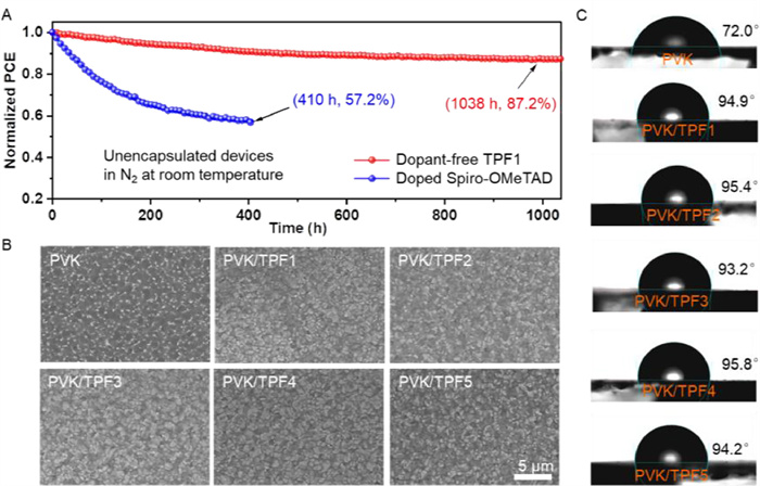
Impressed by high PCE of dopant-free TPF1, we have carefully evaluated its unencapsulated device stability. Fig. S11 (Supporting information) shows that dopant-free TPF1-based PVSC can retain 91.3% of its initial PCE after 1080 h storage under ambient conditions (RH: 30%) at room temperature, which is much better than that of the doped spiro-OMeTAD control device (71.9%). We also measured the device operational stability operated at MPP in N2 at room temperature, and the results are provided in Fig. 6a. It can be easily seen that TPF1-based device presents an impressive operational stability, which retained 87.2% of its initial PCE after 1038 h, while the control device degraded to the 57.2% of its initial PCE after only 410 h operation. We then collected the SEM images of perovskite films covered with and without HTMs, which were aged for 2 days in ambinet conditions. As shown in Fig. 6b, the pure perovskite film shows bright regions in the grain boundaries, which are less observed in the PVK/HTM samples. These bright regions are assigned to the PbI2, originating from the degradation of perovskites induced by the moisture or oxygen [62,63]. These results thus strongly suggest the protective effect from HTMs, which can be further verified by the XRD patterns (Fig. S12 in Supporting information). The water contact angles of the perovskite films covered with and without HTMs are shown in Fig. 6c, showing that the contact angles can increase from 72.0° to over 93° after covering HTMs. The more hydrophobic the surface, the more it will resist moisture, which may be the reason for the protection effect. As a result, the significantly improved device stability of TPF1 is attributed to the absence of dopants, the high thermal stability and the hydrophobic surface [64,65].
In summary, we have successfully designed and synthesized five fluoranthene-cored D-A type branched dopant-free HTMs (TPF1–5) for conventional PVSCs via a facile synthesis. By changing the arm structure, number and substitution sites, the intermolecular interactions, film morphologies, optical properties, energy levels, hole mobilities of the resulting HTMs can be well regulated. Benefiting from the highest hole mobility and favourable film morphology, TPF1 with p-TPA substituted at 7,10-sites shows the best hole extraction/transport ability at the interface, thereby enabling the highest PCE of 21.76% among these dopant-free HTMs. Furthermore, the unencapsulated PVSC based on dopant-free TPF1 performs a much better stability than the doped spiroOMeTAD control device, which retained 87.2% of its initial PCE after MPP tracking for 1038 h in N2 at room temperature. This work thus is a strong confirmation of the feasibility of the D-A type branched structure in the development of efficient and stable HTMs.
The authors declare that they have no known competing financial interests or personal relationships that could have appeared to influence the work reported in this paper.
Xinyu Yu: Investigation, Methodology, Resources, Validation, Writing – original draft, Writing – review & editing. Fei Wu: Investigation, Methodology, Resources, Writing – review & editing. Xianglang Sun: Investigation. Linna Zhu: Project administration, Writing – review & editing. Baoyu Xia: Project administration, Resources, Writing – review & editing. Zhong'an Li: Conceptualization, Funding acquisition, Resources, Supervision, Writing – original draft, Writing – review & editing.
The work was supported by National Key Research & Development Program of China (No. 2023YFE0210900), National Natural Science Foundation of China (No. 21975085), Excellent Youth Foundation of Hubei Scientific Committee (No. 2021CFA065), and open Fund of Hubei Key Laboratory of Material Chemistry and Service Failure (No. 2023MCF02). We would also like to thank the Analytical and Testing Center of HUST for access to their facilities.
Supplementary material associated with this article can be found, in the online version, at doi:
NREL, Best Research-Cell Efficiency Chart, 2023.
L. Zhang, L. Mei, K. Wang, et al., Nano-Micro Lett. 15 (2023) 177. doi: 10.1007/s40820-023-01140-3
J. Park, J. Kim, H.S. Yun, et al., Nature 616 (2023) 724–730. doi: 10.1038/s41586-023-05825-y
C. Li, X. Wang, E. Bi, et al., Science 379 (2023) 690–694. doi: 10.1126/science.ade3970
Y. Mo, C. Wang, X. Zheng, et al., Interdiscip. Mater. 1 (2022) 309–315. doi: 10.1002/idm2.12022
Z. Li, X. Sun, X. Zheng, et al., Science 382 (2023) 284–289. doi: 10.1126/science.ade9637
L. Duan, D. Walter, N. Chang, et al., Nat. Rev. Mater. 8 (2023) 261–281. doi: 10.1038/s41578-022-00521-1
Q. Tan, Z. Li, G. Luo, et al., Nature 620 (2023) 545–551. doi: 10.1038/s41586-023-06207-0
Y. Cai, J. Cui, M. Chen, et al., Adv. Funct. Mater. 31 (2021) 2005776. doi: 10.1002/adfm.202005776
X. Yin, Z. Song, Z. Li, W. Tang, Energy Environ. Sci. 13 (2020) 4057–4086. doi: 10.1039/d0ee02337j
T. Zhang, F. Wang, H.B. Kim, et al., Science 377 (2022) 495–501. doi: 10.1126/science.abo2757
G.W. Kim, H. Choi, M. Kim, et al., Adv. Energy Mater. 10 (2020) 1903403. doi: 10.1002/aenm.201903403
J.Y. Seo, S. Akin, M. Zalibera, et al., Adv. Funct. Mater. 31 (2021) 2102124. doi: 10.1002/adfm.202102124
G. Ren, W. Han, Y. Deng, et al., J. Mater. Chem. A 9 (2021) 4589–4625. doi: 10.1039/d0ta11564a
L. Nakka, Y. Cheng, A.G. Aberle, F. Lin, Adv. Energy Sustain. Res. 3 (2022) 2200045. doi: 10.1002/aesr.202200045
S. Wang, Z. Huang, X. Wang, et al., J. Am. Chem. Soc. 140 (2018) 16720–16730. doi: 10.1021/jacs.8b09809
Y. Liu, Y. Hu, X. Zhang, et al., Nano Energy 70 (2020) 104483. doi: 10.1016/j.nanoen.2020.104483
Y. Shen, K. Deng, Q. Chen, et al., Adv. Mater. 34 (2022) 2200978. doi: 10.1002/adma.202200978
L. Yuan, W. Zhu, Y. Zhang, et al., Energy Environ. Sci. 16 (2023) 1597–1609. doi: 10.1039/d2ee03565k
X.L. Sun, D.B. Zhao, Z.A. Li, Chin. Chem. Lett. 29 (2018) 219–231. doi: 10.1016/j.cclet.2017.09.038
P. Yan, D. Yang, H. Wang, et al., Energy Environ. Sci. 15 (2022) 3630–3669. doi: 10.1039/d2ee01256a
G. Xie, J. Chen, H. Li, et al., Chin. J. Chem. 41 (2023) 3133–3166. doi: 10.1002/cjoc.202300234
L. Shao, F. Tong, M. Zhu, et al., Chin. Chem. Lett. 31 (2020) 2452–2458. doi: 10.1016/j.cclet.2020.03.036
Y.D. Wang, Y. Wang, J.Y. Shao, et al., ACS Energy Lett. 6 (2021) 2030–2037. doi: 10.1021/acsenergylett.1c00531
S. Daskeviciute-Geguziene, Y. Zhang, K. Rakstys, et al., Adv. Funct. Mater. 33 (2023) 2208317. doi: 10.1002/adfm.202208317
Q. Cheng, H. Chen, F. Yang, et al., Angew. Chem. Int. Ed. 61 (2022) e202210613. doi: 10.1002/anie.202210613
C. Shen, Y. Wu, H. Zhang, et al., Angew. Chem. Int. Ed. 58 (2019) 3784–3789. doi: 10.1002/anie.201811593
A. Jegorove, J. Xia, M. Steponaitis, et al., Chem. Mater. 35 (2023) 5914–5923. · doi: 10.1021/acs.chemmater.3c00708
Y. Zhou, L. Ding, K. Shi, et al., Adv. Mater. 24 (2012) 957–961. doi: 10.1002/adma.201103927
L. Ding, C.Y. Yang, Y.Q. Zheng, et al., Asian J. Org. Chem. 6 (2017) 1231–1234. doi: 10.1002/ajoc.201700203
X. Sun, Q. Xue, Z. Zhu, et al., Chem. Sci. 9 (2018) 2698–2704. doi: 10.1039/c7sc05484j
X. Yu, Z. Li, X. Sun, et al., Nano Energy 82 (2021) 105701. doi: 10.1016/j.nanoen.2020.105701
H.D. Pham, T.T. Do, J. Kim, et al., Adv. Energy Mater. 8 (2018) 1703007. doi: 10.1002/aenm.201703007
N.J. Jeon, H.G. Lee, Y.C. Kim, et al., J. Am. Chem. Soc. 136 (2014) 7837–7840. doi: 10.1021/ja502824c
R. Azmi, S.Y. Nam, S. Sinaga, et al., Nano Energy 44 (2018) 191–198. doi: 10.1016/j.nanoen.2017.12.002
C.M. Cardona, W. Li, A.E. Kaifer, et al., Adv. Mater. 23 (2011) 2367–2371. doi: 10.1002/adma.201004554
J. Sworakowski, Synth. Met. 235 (2018) 125–130. doi: 10.1016/j.synthmet.2017.11.013
C. Wang, L. Ouyang, X. Xu, et al., Sol. RRL 2 (2018) 1800122. doi: 10.1002/solr.201800122
N.J. Jeon, H. Na, E.H. Jung, et al., Nat. Energy 3 (2018) 682–689. doi: 10.1038/s41560-018-0200-6
Y. Wang, W. Chen, L. Wang, et al., Adv. Mater. 31 (2019) 1902781. doi: 10.1002/adma.201902781
M. Cekaviciute, J. Simokaitiene, G. Sych, et al., Dyes Pigm. 134 (2016) 593–600. doi: 10.1016/j.dyepig.2016.08.007
F. Liu, F. Wu, W. Ling, et al., ACS Energy Lett. 4 (2019) 2514–2521. doi: 10.1021/acsenergylett.9b01539
F.J. Ramos, K. Rakstys, S. Kazim, et al., RSC Adv. 5 (2015) 53426–53432. doi: 10.1039/C5RA06876B
Y. Wei, Y. Zhang, Y. Ren, et al., Adv. Funct. Mater. 33 (2023) 2307501. doi: 10.1002/adfm.202307501
A. Magomedov, S. Paek, P. Gratia, et al., Adv. Funct. Mater. 28 (2018) 1704351. doi: 10.1002/adfm.201704351
A. Zheng, J. Wang, N. Xu, et al., ACS Photonics 5 (2018) 4694–4701. doi: 10.1021/acsphotonics.8b01336
H. Lu, F. Wu, Y. Yang, et al., J. Mater. Chem. C 8 (2020) 13415–13421. doi: 10.1039/d0tc03404e
M. Jeong, I.W. Choi, K. Yim, et al., Nat. Photonics 16 (2022) 119–125. doi: 10.1038/s41566-021-00931-7
M. Stolterfoht, C.M. Wolff, J.A. Márquez, et al., Nat. Energy 3 (2018) 847–854. doi: 10.1038/s41560-018-0219-8
M. Stolterfoht, P. Caprioglio, C.M. Wolff, et al., Energy Environ. Sci. 12 (2019) 2778–2788. doi: 10.1039/c9ee02020a
Z. Jiang, T. Du, C.T. Lin, et al., Adv. Mater. Interfaces 10 (2023) 2201737. doi: 10.1002/admi.202201737
J.W. Lee, S.G. Kim, S.H. Bae, et al., Nano Lett. 17 (2017) 4270–4276. doi: 10.1021/acs.nanolett.7b01211
D.S. Lee, J.S. Yun, J. Kim, et al., ACS Energy Lett. 3 (2018) 647–654. doi: 10.1021/acsenergylett.8b00121
Q. Chen, H. Zhou, T.B. Song, et al., Nano Lett. 14 (2014) 4158–4163. doi: 10.1021/nl501838y
S. Kanaya, G.M. Kim, M. Ikegami, et al., J. Phys. Chem. Lett. 10 (2019) 6990–6995. doi: 10.1021/acs.jpclett.9b02665
E.V. Péan, S. Dimitrov, C.S. De Castro, M.L. Davies, Phys. Chem. Chem. Phys. 22 (2020) 28345–28358. doi: 10.1039/d0cp04950f
E.A. Alharbi, A. Krishna, T.P. Baumeler, et al., ACS Energy Lett. 6 (2021) 3650–3660. doi: 10.1021/acsenergylett.1c01754
K. Jiang, J. Wang, F. Wu, et al., Adv. Mater. 32 (2020) 1908011. doi: 10.1002/adma.201908011
Q. Fu, Z. Xu, X. Tang, et al., ACS Energy Lett. 6 (2021) 1521–1532. doi: 10.1021/acsenergylett.1c00385
X. Ji, T. Zhou, Q. Fu, et al., Adv. Energy Mater. 13 (2023) 2203756. doi: 10.1002/aenm.202203756
Y. Bai, Z. Zhou, Q. Xue, et al., Adv. Mater. 34 (2022) 2110587. doi: 10.1002/adma.202110587
X. Deng, F. Qi, F. Li, et al., Angew. Chem. Int. Ed. 61 (2022) e202203088. doi: 10.1002/anie.202203088
R.K. Battula, G. Veerappan, P. Bhyrappa, et al., RSC Adv. 10 (2020) 30767–30775. doi: 10.1039/d0ra05590e
G. Qu, L. Dong, Y. Qiao, et al., Adv. Funct. Mater. 32 (2022) 2206585. doi: 10.1002/adfm.202206585
Q. Fu, X. Tang, H. Liu, et al., J. Am. Chem. Soc. 144 (2022) 9500–9509. doi: 10.1021/jacs.2c04029

Figure 2 Calculated geometry structure and electrostatic potential distribution of TPF1–3.

Figure 3 Absorption spectra of TPF1–5 in dichloromethane solutions (A) and films (B). (C) CV curves of TPF1–5 in film state. (D) DSC curves of TPF1–5 measured under nitrogen at a heating rate of 10 ℃/min. (E) XRD patterns of TPF1–5 powders. (F) The hole injection characteristics measured by the SCLC method based on a device structure of ITO/PEDOT: PSS/HTM/MoO3/Ag.

Figure 4 (A) The device structure of n-i-p PVSCs. (B) Energy alignment of components in devices. (C) J-V curves of the best performing PVSCs based on dopant-free TPF1–5. (D) J-V curves with different scan directions in PVSCs based on dopant-free TPF1. (E) Stable output current and PCE of the dopant-free TPF1-based device under a constant bias of 0.97 V. (F) EQE spectra with the integrated short-circuit current density for champion devices.

Figure 5 (A) Steady-state PL spectra and (B) time-resolved PL spectra of perovskite films covered with and without HTMs. (C) Transient photocurrent decay curves and (D) transient photovoltage decay curves of devices based on TPF1–5 with decay time noted.

Figure 6 (A) Device stability of unencapsulated devices based on dopant-free TPF1 and doped spiroOMeTAD under MPP tracking in N2 atmosphere at room temperature. (B) SEM images and (C) contact angles with respect to water of perovskite films covered with and without HTMs. Note: all SEM images use the same scale bar as in PVK/TPF5.
Table 2. Device parameters of the n-i-p PVSCs based on dopant-free TPF1–5 and doped Spiro-OMeTAD.
|
|
 下载: 导出CSV

 扫一扫看文章

扫一扫关注我们


 下载:
下载: