MIIT Key Laboratory of Critical Materials Technology for New Energy Conversion and Storage, School of Chemistry and Chemical Engineering, Harbin Institute of Technology, Harbin 150001, China
* Corresponding author. E-mail address: pxu@hit.edu.cn (P. Xu). 1 These authors contributed equally to this work.
Received Date:
02 September 2023 Accepted Date:
14 November 2023 Revised Date:
24 September 2023 Available Online:
15 September 2024
Abstract:
Surface-enhanced Raman scattering (SERS) spectroscopy has emerged as a powerful analytical technique for detecting and identifying trace chemical and biological molecules. In this review, we present an in-depth discussion of recent advances in the field of crystal phase manipulation to achieve exceptional SERS performance. Focusing on transition metal dichalcogenides, (hydr)oxides, and carbides as exemplary materials, we illustrate the pivotal role of crystal phase regulation in enhancing SERS signals. By exploring the correlation between crystal phases and SERS responses, we uncover the underlying principles behind these strategies, thereby shedding light on their potential for future SERS applications. By addressing the current challenges and limitations, we also propose the prospects of the crystal phase strategy to facilitate the development of cutting-edge SERS-based sensing technologies.
Surface-enhanced Raman scattering (SERS) spectroscopy has emerged as a highly sensitive and efficient analytical detection technique with remarkable advantages, including simplicity, rapidity, and non-destructiveness [1–3]. It has wide application in diverse fields, such as drug detection, environmental monitoring, food safety, chemical and biological sensing, and medical diagnostics [4–7]. The phenomenon of Raman scattering, discovered by the Indian scientist Chandrasekhara Venkata Raman in 1928, refers to the inelastic scattering of light [8]. However, conventional Raman spectroscopy suffers from low signal intensity, limiting its applicability to solid samples or high-concentration solutions. In 1974, Fleischmann et al. observed the enhanced Raman signal of pyridine molecules on a roughened silver electrode surface [9]. In 1977, Van Duyne et al. proposed the electromagnetic (physical) enhancement mechanism which effectively explained the Raman enhancement on silver electrodes; the term 'surface-enhanced Raman scattering' (SERS) originates from this mechanism [10]. At present, two mechanisms are widely accepted to account for SERS phenomenon: the aforementioned electromagnetic enhancement mechanism and the chemical enhancement mechanism [11–13]. The former stems from the surface plasmon resonance effect induced by incident light on noble metal surfaces [14,15], while the latter is mainly due to charge transfer between the substrate and adsorbed molecules [16]. Traditionally, noble metals (e.g., Au, Ag, and Cu) have dominated this field due to their high-sensitivity SERS responses [17–19]. However, the widespread application of noble metal substrates may be hindered by inherent drawbacks such as high cost, complex regulation of 'hot spots', strong spectral backgrounds, and various side effects [20–23]. By contrast, non-noble metal substrates possess advantages such as abundant sources, low prices, tunable electronic structures, and unique selectivity towards target molecules [24–26]. These characteristics compensate for the limitations of noble metal substrates, thereby significantly expanding the scope of SERS applications. Nevertheless, non-noble metal substrates have inferior SERS performance compared to the noble metal substrates as chemical enhancement is usually several orders of magnitude lower than electromagnetic enhancement. Therefore, improving the SERS performance of non-noble metal substrates has become a prominent research area.
The crystal phase of non-noble metal substrates plays a pivotal role in determining their properties and functionalities [27]. Thus, the crystal phase should be considered as a significant structural parameter, in addition to composition, morphology, architecture, facet, size, and dimensionality [27]. Materials can exist in various crystalline and amorphous phases, with the former exhibiting ordered atomic arrangements and the latter featuring a disordered arrangement of atoms [28]. Although the dominant crystal phase of a material is primarily influenced by atomic bonding and thermodynamic parameters, many materials can possess multiple crystal phases [29]. In particular, fine-tuning experimental conditions has made it possible to control the structural parameters of nanomaterials and achieve thermodynamically less favorable crystal phases [30]. Materials with different crystal phases often have very distinct physicochemical properties, including charge distribution, Fermi level, band gap and density of state [31]. Therefore, manipulating the crystal phase or inducing phase transitions offers a promising approach to significantly improve the SERS sensitivity of non-noble metal substrates.
In this review, we focus on recent advances in crystal phase-induced strategy for improving the SERS performance. Specifically, we take transition metal dichalcogenides (TMDs), transition metal (hydr)oxides (TMOs) and transition metal carbides (TMCs) as examples to illustrate the significance of crystal phase manipulation in achieving superior SERS performance. By analyzing the correlation between crystal phases and SERS performance, we aim to provide insights into the fundamental principles underlying these strategies and evaluate their potential for future SERS applications. Furthermore, we point out the current limitations and prospects of crystal phase manipulation to facilitate the development of advanced SERS-based sensing technologies.
2.
Transition metal dichalcogenides (TMDs)
As a typical group of polymorphic materials, TMDs have emerged as promising materials due to their wide range of optical, thermal and electronic properties, which can be considerably influenced by their crystal phases [32–34]. Crystal phases, such as 2H, 1T, 1T', and 3R, exhibited by TMDs (Figs. 1a–f) have potential in boosting the SERS performance [35].
Figure 1
Figure 1.
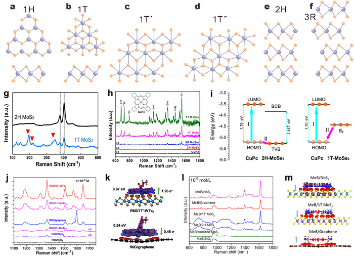
(a–f) Schematic illustration of common crystal phase structure of TMD materials. Reproduced with permission [35]. Copyright 2019, Science China Press and Springer Nature. (g) Raman evidence of crystal phase transition of the MoS2 substrate. (h) Comparison of SERS activity between 2H-MoS2, 2H-MoSe2, 1T-MoS2, and 1T-MoSe2 substrates using CuPc as the probe. (i) Schematic illustration of the charge transfer process between 2H-MoSe2 and 1T-MoSe2 monolayers and CuPc molecule. Reproduced with permission [36]. Copyright 2017, Wiley-VCH. (j) Comparison of SERS activity between 1T'-WTe2 and other common two-dimensional materials. (k) Charge distribution difference for R6G adsorbed on 1T'-WTe2 and graphene for comparation. Reproduced with permission [43]. Copyright 2018, American Chemical Society. (l) Comparison of SERS activity between NbS2 and other common two-dimensional materials. (m) Charge distribution difference for MB adsorbed on NbS2, 1T-MoS2 and graphene for comparation. Reproduced with permission [44]. Copyright 2019, American Chemical Society.
Our group conducted a systematic study on the SERS performance of single-layer MoX2 (X = S, Se) with different phases to investigate the relationship between the crystal phases of TMDs and the SERS effect [36]. In contrast to our previously developed methods of liquid ammonia lithiation and deep hydrothermal reduction employed for energy conversion [37,38], a different synthesis strategy was employed in the SERS research. In particular, 2H-phase MoX2 (X = S, Se) monolayers were obtained by ultrasonically exfoliating bulk 2H-phase materials in N-methyl-2-pyrrolidone. Meanwhile, 1T-phase MoX2 (X = S, Se) monolayers were obtained by intercalating n-butyl lithium and ultrasonically exfoliating the 2H-phase bulk material, resulting in crystal phase transition (Fig. 1g). This method not only offers improved simplicity in synthesis, but also ensures a consistent morphology between 1T-phase and 2H-phase samples, which are single-layer nanosheets. Using thermally evaporated copper phthalocyanine (CuPc) and solution adsorbed rhodamine 6G (R6G) and crystal violet (CV) as probe molecules, it was observed that 1T-phase MoX2 (X = S, Se) substrates exhibited stronger SERS response than 2H-phase MoX2 (X = S, Se) substrates, with the enhancement sequence of 1T-MoSe2 > 1T-MoS2 > 2H-MoSe2 > 2H-MoS2 (Fig. 1h). A series of experimental investigations and theoretical calculations were conducted. UV–vis absorption spectra revealed the absence of surface plasmon resonance bands in the visible light region, thereby excluding electromagnetic enhancement as a contributing factor for these materials. Pronounced wavelength-dependent SERS responses were observed, suggesting that the SERS performance was due to charge transfer-related chemical enhancement. Density functional theory (DFT) calculations were performed to reveal the electronic band structures of the materials. 2H-phase MoX2 (X = S, Se) substrates belong to the semiconducting phases, whereas 1T-phase MoX2 (X = S, Se) substrates exhibit characteristics of metallic phases. A reasonable charge transfer-based chemical enhancement mechanism was proposed based on the results (Fig. 1i). The charge transfer process between the substrate and the adsorbed molecule proceeds in two steps. First, under the excitation of incident light, electrons at the highest occupied molecular orbital (HOMO) level of the probe molecule are excited to the lowest unoccupied molecular orbital (LUMO) level. Second, electrons at the tail valence band (TVB) or Fermi level of the substrate transfer to the HOMO level of the molecule, thereby increasing the Raman scattering cross-section of the molecule and affording SERS signals. Unlike 2H-phase MoX2 (X = S, Se), the Fermi level of 1T-phase MoX2 (X = S, Se) is higher than the HOMO level of the probe molecule, so the charge transition from the Fermi level of 1T-phase MoX2 (X = S, Se) to the HOMO level of the molecule does not require additional energy, thereby increasing the probability of charge transfer between the substrate and molecule. Therefore, 1T-phase MoX2 (X = S, Se) materials have stronger Raman enhancement ability than 2H-phase MoX2 (X = S, Se). To the best of our knowledge, this work was the first to apply a crystal phase transition strategy to realize remarkable SERS performance, laying a solid foundation for the exploration and utilization of 1T-phase TMDs in SERS applications.
Subsequently, other 1T-phase TMDs with great potential in SERS applications were reported. For example, Zhang et al. successfully synthesized large-scale 1T-SnSe2 thin films by a facile chemical vapor deposition (CVD) technique using SnSe and Se powders as precursors. The 1T-SnSe2 substrate demonstrates good sensitivity in detecting common dyes at concentrations as low as 10−8 mol/L [39]. Furthermore, Qiu et al. investigated the SERS activity of 1T-PtSe2 with varying numbers of layers [40]. It was observed that the SERS performance of 1T-phase PtSe2 decreases significantly with increasing layer numbers. Through mechanism experiments and DFT calculations, this phenomenon could be attributed to the strong interlayer interaction of 1T-PtSe2, leading to a significant reduction of its band gap with the increasing number of layers and results in a mismatch of the energy level with the probe molecule. Moreover, Li et al. prepared 1T-phase HfTe2 nanosheets through the combination of liquid exfoliation and hydrothermal method and detected the SERS of R6G molecules with concentrations ranging from 10−3 mol/L to 10−9 mol/L [41]. The observed SERS activity of 1T-HfTe2 nanosheets could be attributed to the charge transfer resonance process between the valence band of HfTe2 and the LUMO of the dye molecules because the energy required for electron-excited transition between them matched well with the energy excitation of the laser. The HfTe2 substrate was further used to detect of uric acid, an essential biomarker of gout disease, with a detection limit of 100 µmol/L, demonstrating the potential of the 1T-HfTe2 substrate for nanodiagnosis.
Our group also demonstrated the SERS effect of single and multi-layer 1T'-phase ReS2 films prepared by CVD [42]. The strong layer-dependent SERS effect of the ReS2 substrate was observed with CuPc as the probe molecule. Several dye molecules (R6G, methylene blue (MB), CV, and rhodamine B (RhB)) were further employed to examine the detection ability of single-layer ReS2, which demonstrated a detection limit as low as 10−9 mol/L. A 5 nm Al2O3 dielectric layer was deposited on the surface of the ReS2 film through atomic layer deposition to prevent the charge transfer between the ReS2 substrate and the adsorbed molecule. The R6G Raman signals was not detected on the Al2O3 covered ReS2 film but was strong on the bare ReS2 film. Regardless of the existence of the Al2O3 dielectric layer, the fluorescence quenching effect became more pronounced with increasing number of ReS2 layers. Hence, the SERS effect on the ReS2 substrate originated from charge transfer, instead of energy transfer. This work not only confirmed the excellent SERS performance potential of 1T'-phase TMDs but also provided new ideas for studying the SERS mechanism.
Tao and co-workers reported 1T'-W(Mo)Te2 as a highly sensitive SERS platform, and the SERS sensitivities of common dyes on 1T'-W(Mo)Te2 reached those of noble metal counterparts and increased when integrated with a Bragg reflector (Figs. 1j and k) [43]. The SERS signals of R6G can be detected even at ultralow concentrations of 4 × 10⁻¹⁴ mol/L (4 × 10⁻¹³ mol/L) on pristine 1T'-W(Mo)Te2. When combined with the Bragg reflector, the limit of detection was further improved to 4 × 10⁻¹⁵ mol/L (4 × 10⁻¹⁴ mol/L). Mechanism experiments and theoretical calculations strongly indicated that the analyte exhibited a robust interaction with 1T'-W(Mo)Te2. Additionally, semimetal 1T'-W(Mo)Te2 exhibited a high density of states near the Fermi level. These combined factors contributed to the observed remarkable SERS effects.
Apart from 1T and 1T'-phases, the SERS effect of TMDs with other phases was investigated. Song et al. demonstrated that mixed-phase (2H+3R) NbS2 is an excellent SERS substrate, with a detection limit of as low as 10−14 mol/L (Figs. 1l and m) [44]. DFT calculations revealed that compared with other 2D substrates, such as 1T-MoS2 and graphene, the NbS2 substrate had the strongest binding energy with the probe molecule and the highest electronic density of states near the Fermi level, resulting in the highest SERS response. As a practical application, the NbS2 substrate was successfully applied to distinguish different types of red wines, enabling direct, rapid, and reliable detection in real life. On this basis, Lv et al. investigated the SERS effect of mixed-phase (2H+3R) NbSe2 [45]. Unlike the layer-dependent SERS effect of other TMD substrates, the SERS activity of NbSe2 reached its maximum at a thickness of six layers, with a low detection limit of 5 × 10⁻¹⁶ mol/L for the analyte molecule. This distinct thickness-dependent effect was attributed to the strong interlayer coupling in NbSe2, which led to the highest adsorption energy and charge transition probability with the adsorbed molecule when the NbSe2 substrate thickness was six layers.
Pioneering works on TMDs have demonstrated that the crystal phase plays a crucial role in their SERS performance, which offers valuable insights into designing and fabricating high-performance SERS substrates. By manipulating and controlling the crystal phase of TMDs, it is now possible to design SERS substrates with tailored properties, enabling the development of highly efficient and sensitive platforms for various applications.
3.
Transition metal (hydr)oxides (TMOs)
TMOs are abundant in nature and play a critical role in the SERS field [46]. Nickel oxide is the first non-noble metal SERS material discovered [47]. However, pristine TMOs typically exhibit insignificant SERS activity, highlighting the critical need for crystal phase manipulation.
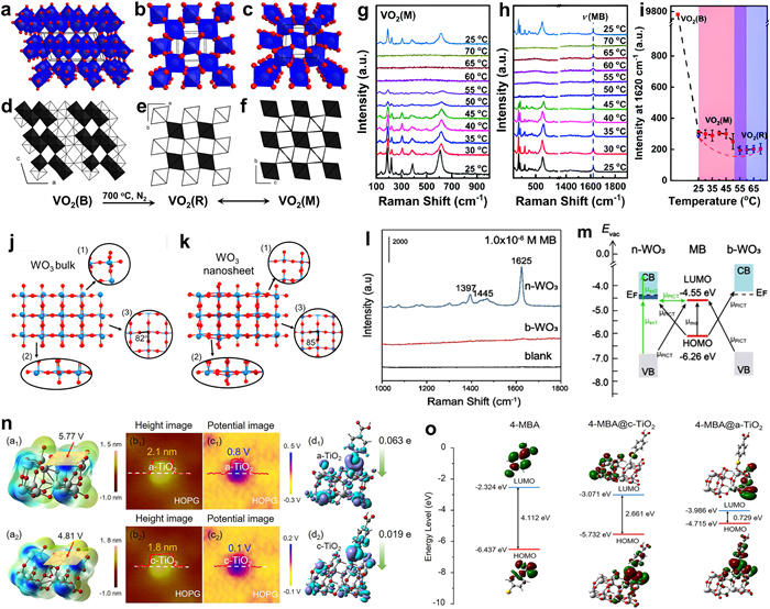
Vanadium oxides possess a wide variety of crystal structures due to the rich oxidation state of vanadium and the strong ability of the vanadium oxide octahedral structure to accommodate point defects. This unique property of vanadium oxides makes them ideal models for the study of crystal phase-dependent SESR activity. Using VO2 nanosheets with different phase structures as an example, our group investigated the influence of the crystal phase of the transition metal oxide on the SERS performance [48]. Three representative phases of VO2 are illustrated in Figs. 2a–f. Monoclinic VO2(B), a metastable phase, was produced by a hydrothermal method and can be irreversibly transformed into a highly-ordered tetragonal rutile VO2(R) phase by annealing at 700 ℃. VO2(R) can be further transformed into a monoclinic deformed VO2(M) phase by a reversible crystal phase transition after cooling to ambient temperature. Among the three crystal phases, VO2(B) has the lowest symmetry, VO2(R) has the highest and VO2(M) has the medium.
Figure 2
Figure 2.
(a–f) Schematic illustration of crystal structures and projection images of the monoclinic VO2(B), rutile VO2(R), and monoclinic deformed VO2(M). (g) Raman spectra of the reversible crystal phase transition process between VO2(M) and VO2(R). (h) SERS spectra of 10−5 mol/L MB during the crystal phase transition process between VO2(M) and VO2(R). (i) Crystal phase-dependent Raman intensity at 1620 cm−1 peak of MB molecules on three different crystal phases of VO2 substrates. Reproduced with permission [48]. Copyright 2018, Royal Society of Chemistry. Schematic illustration of crystal structures of (j) WO3 bulk and (k) WO3 nanosheets. (l) Comparison of SERS activity between WO3 bulk and WO3 nanosheets. (m) Schematic illustration of the charge transfer process between WO3 bulk and WO3 nanosheets and MB molecule. Reproduced with permission [49]. Copyright 2020, Wiley-VCH. (n) Calculated ESP, AFM images and KPFM-measured surface potential images for c-TiO2 and a-TiO2, and charge distribution difference for 4-MBA adsorbed on a-TiO2 and c-TiO2 substrates. (o) Schematic illustration of the energy band of 4-MBA, and 4-MBA adsorbed on c-TiO2 and a-TiO2. Reproduced with permission [51]. Copyright 2019, American Chemical Society.
XRD and Raman analyses confirmed the crystal phase transition from VO2(B) to VO2(M). The reversible crystal phase transition between VO2(M) and VO2(R) was also proved by Raman spectra (Fig. 2g). The Raman peaks of VO2(M) can be clearly observed at low temperatures; when heated to 60 ℃, the peaks of the material suddenly disappeared, indicating the crystal phase transition from VO2(M) to VO2(R). When the temperature was cooled down to room temperature, the Raman peaks returned to those of VO2(M), suggesting that the crystal phase transition was reversible. MB was chosen as the probe molecule to investigate the influence of the crystal phase of VO2 nanosheets on SERS performance. As shown in Figs. 2h and i, the VO2(B) substrate exhibits the strongest SERS effect, which is about 30 times higher than that of the VO2(M) substrate (Fig. 2i). In particular, the comparison of SERS performance between VO2(M) and VO2(R) was investigated in situ by using a temperature control device (Linkam THMS600) (Fig. 2h). When VO2(M) was converted into VO2(R) upon heating, the SERS activity of the substrate gradually decreased. Upon cooling to room temperature, the SERS activity was restored as the substrate reverted to VO2(M). All the results clearly showed that the crystal phase transition from VO2(B) to VO2(M) and then to VO2(R) significantly affected the SERS activity of VO2 substrates in the following order: VO2(B) > VO2(M) > VO2(R). The photoluminescence signal of R6G was significantly quenched on VO2 nanosheets, and the resonant Raman enhancement effect was observed on the VO2 substrates similar to that on TMD materials. As such, the SERS origin of VO2 substrates was assigned to the charge transfer-based chemical enhancement rather than electromagnetic enhancement. The high symmetry lattice of the crystal of non-noble metal SERS substrates limits the charge transfer and vibrational coupling between the substrate and the adsorbed molecule, resulting in a decrease in the SERS response. The crystal structures and projection images of VO2(B), VO2(M) and VO2(R) were analyzed to better understand the difference in the SERS activity of VO2 nanosheets with different crystal phases. As shown in Figs. 2a–f, VO2(B) crystallizes in the monoclinic C2/m space group and adopts an anisotropic laminar arrangement with parallel quadrilateral axes. The VO6 octahedron in VO2(B) is deformed because V4+ deviates from the center of the VO6 octahedron, resulting in two different types of VO6 octahedrons (with two inequivalent V4+ sites and four inequivalent O2− sites) in VO2(B). In the low-dimensional nanosheet structure, the periodic presence of oxygen vacancies further reduces the crystal symmetry in the VO2(B) crystal structure. Therefore, VO2(B) is highly disordered and asymmetric. VO2(R) has a rutile structure and crystallizes in the tetragonal P42/mnm space group. V4+ is located at the center of the regular VO6 octahedron and bonded to six equivalent O2− atoms, making VO2(B) highly symmetric. VO2(M) is slightly deformed from VO2(R) and belongs to the tetragonal P42/mnm space group, in which two inequivalent O2− atoms are each bonded to three equivalent V4+ atoms, resulting in a moderately symmetrical structure compared to VO2(B) and VO2(R). Therefore, VO2(B) exhibits the best SERS performance among the three VO2 substrates due to its lowest crystal symmetry. Besides, the oxygen vacancies on the surface of VO2(B) further enrich the surface defect states and enhance the charge transfer between the substrate and the adsorbed molecules. The significant decrease in the SERS activity of VO2(M) nanosheets compared to VO2(B) is due to the increase in crystal symmetry after the crystal phase transition and the reduction of surface defects caused by high-temperature annealing. Moreover, the transformation of VO2(M) to VO2(R) improves the crystal symmetry, which also reduces the SERS performance. The study of the SERS effect of the VO2 substrates once again proved that the crystal phase of SERS substrates has a direct influence on SERS.
Recent research by Zhao and co-workers supported our results [49]. In their study, ultrathin WO3 nanosheets (monoclinic deformed phase, the same as our VO2(M)) were utilized as a prototype material to demonstrate the role of surface defects in inducing strong charge transfer interactions at the substrate−molecule interface, resulting in a remarkable 100-fold improvement in SERS activity (Figs. 2j–l). In particular, the downsizing of WO3 bulk into ultrathin nanosheets for SERS-active substrates intrinsically altered the surface and band energy structures of WO3, which in turn, modified the electronic structure of the nanosheets and their interactions with probe molecules; this phenomenon ultimately led to the creation of new charge transfer pathways that enabled more sensitive SERS detection of probe molecules (Fig. 2m). In comparison with SERS-inactive WO3 bulk materials, the degree of charge transfer for MB molecules on WO3 nanosheets was significantly higher, estimated to be 0.89 versus 0.55 on WO3 bulk, indicating that the enhanced charge transfer contribution from surface defects is the primary factor responsible for the increased SERS activity of WO3 nanosheets.
Amorphous materials with numerous defects have a long-range disordered structure with many dangling bonds and band tails that contribute to their existence in a metastable state. This state could facilitate surface charge escape and transfer, leading to remarkable SERS activity. Guo and co-workers compared amorphous ZnO nanocages (a-ZnO) and crystalline ZnO nanocages (c-ZnO) [50]. a-ZnO exhibited an ultrahigh SERS activity, surpassing that of c-ZnO. The DFT calculations suggested that high-efficiency interfacial charge transfer between the a-ZnO and the probe molecule was responsible for this phenomenon due to the metastable electronic states of a-ZnO. Moreover, X-ray absorption near-edge structure (XANES) characterization verified that efficient charge transfer could generate π bonding in Zn-S bonds peculiar to the mercapto molecule-adsorbed a-ZnO substrates. Guo and co-workers also developed amorphous TiO2 nanosheets (a-TiO2) with high-efficiency photoinduced charge transfer for excellent SERS activity (Figs. 2n and o) [51]. a-TiO2 possessed a more positive surface potential than their crystalline counterparts (c-TiO2), allowing for significant charge transfer from the adsorbed molecule to a-TiO2 and facilitating the formation of a stable surface charge-transfer complex (Fig. 2n). In addition, the smaller band gap and higher electronic density of states of a-TiO2 effectively increased the vibronic coupling of resonances in the substrate–molecule system, leading to remarkable SERS activity of a-TiO2 (Fig. 2o).
Attracted by the superiority of the amorphous phase, our group also developed a series of amorphous SERS substrates, including amorphous Fe(OH)3, Co(OH)2, and Ni(OH)2 octahedral microcages [52]. Ni(OH)2 microcages provided the optimal SERS activity of various probe molecules due to the strongest coupling interactions between the molecule and metal center, which greatly facilitated the charge transfer. Our findings indicated that amorphous hydroxides do not need to be converted into oxides to serve as highly active SERS substrates, which not only eliminates the annealing process but also provides better SERS performance.
Our conclusion was further supported by Guo and co-workers, who reported that amorphous Zn(OH)2 (a-Zn(OH)2) exhibited higher SERS sensitivity than amorphous ZnO (a-ZnO) due to the abundant O atoms and enriched O 2p state density near the Fermi level in a-Zn(OH)2, leading to higher charge transfer probabilities [53]. Additionally, a-Zn(OH)2 exhibits significant advantages in energy-level matching over a-ZnO for efficient photoinduced charge transfer through strong vibronic coupling due to the upshifted valence band maximum and narrow band gap of a-Zn(OH)2.
Research on the SERS effects of TMOs has steadily advanced over time, and crystal phase manipulation can significantly affect their SERS activity. According to pioneering works, the transformations from high symmetry to low symmetry, from low defect to high defect, and from crystalline to amorphous phases of TMOs can lead to significant enhancements in SERS activity, paving the way for the development of high-performance TMOs-based SERS substrates.
4.
Transition metal carbides (TMCs)
TMCs are composed of a transition metal atom bonded to one or more carbon atoms and have received considerable attention in the scientific and technological communities. Unlike TMDs that involve crystal phase transitions between metallic and semiconducting phases, and TMOs that exhibit crystal phase transitions between semiconducting and semiconducting phases, TMCs represent a class of exemplary quasi-metallic materials that are suitable for investigating the influence of different metallic crystal phases on the SERS effect [54–56]. Our group conducted a systematic study using α-MoC and β-Mo2C as the research models (Figs. 3a–c) [57]. As depicted in Fig. 3a, α-MoC has a face-centered cubic structure while β-Mo2Cadopts a hexagonal close-packed structure. To compare the SERS performance of these two crystal phases, we used R6G, CV, and MB as probe molecules. The SERS activity of β-Mo2C was two to four times higher than that of α-MoC, illustrating the substantial influence of the crystal phase on the SERS response. A series of experiments and theoretical calculations were conducted to understand the SERS mechanism of the different crystal phases of molybdenum carbides. Notably, although DFT calculations revealed that both α-MoC and β-Mo2C exhibit typical characteristics of metallic phases, no plasmon resonance peak was observed in the UV–vis absorption spectra within the visible region. This finding rules out the contribution of electromagnetic enhancement. A wavelength-dependent SERS intensity was observed, implying the involvement of charge transfer-based chemical enhancement. This finding was further supported by the presence of enhanced non-totally symmetric b2 modes in the spectrum. Additionally, the absorption peak of MB in the UV–vis spectra showed broadening and significant redshift after adsorption onto α-MoC and β-Mo2C substrates, suggesting the presence of a new charge transfer process. Overall, these results indicate that the SERS effect of the molybdenum carbide substrates could be due to charge transfer-based chemical enhancement instead of electromagnetic enhancement. The charge difference distributions for MB adsorbed α-MoC and β-Mo2C were calculated using DFT to explain the discrepancy in SERS activity among different crystal phases of molybdenum carbides. α-MoC and β-Mo2C experience a gain in charge upon MB adsorption, but β-Mo2C exhibits a more efficient charge transfer compared with α-MoC. This was supported by XPS analysis, as the Mo 3d peak of β-Mo2C displayed a more pronounced shift towards low binding energy after MB adsorption than α-MoC. The photoinduced charge transfer diagram between the two substrates and the probe molecule is shown in Fig. 3c, in which the Fermi levels of α-MoC and β-Mo2C were determined to be 4.85 eV and 4.73 eV by using Kelvin probe force microscopy. The Fermi level of β-Mo2C exhibits a nearly symmetric alignment with the HOMO and LUMO of MB molecule, making it more favorable for the photoinduced charge transfer process. Furthermore, the density of states of α-MoC and β-Mo2C were calculated and compared. According to Fermi's golden rule, the density of states near the Fermi level strongly affects the probability of the charge transfer between the SERS substrate and the probe molecule. As shown in Fig. 3b, β-Mo2C has a higher density of states near the Fermi level than α-MoC. This finding suggests that β-Mo2C has a higher probability of charge transfer with the probe molecule, leading to better SERS activity than α-MoC. Our work indicated that even though the different crystal phases of the TMCs are metallic, crystal phase manipulation is still very important.
Figure 3
Figure 3.
(a) Schematic illustration of crystal structures of α-MoC and β-Mo2C. (b) Comparison of the density of states of α-MoC and β-Mo2C substates. (c) Schematic illustration of the charge transfer process between α-MoC and β-Mo2C substrates and MB molecule. Reproduced with permission [57]. Copyright 2022, Royal Society of Chemistry. (d) Density of states and (e) electronic local function of the WCx substrate. (f) SERS spectra of 10−5 mol/L R6G obtained on WCx chip, Ag chip, and Si wafer. Reproduced with permission [60]. Copyright 2020, Royal Society of Chemistry. (g) Schematic illustration of the Ti3C2 substrates. (h) Charge distribution difference of R6G adsorbed on the Ti3C2 surface. (i) SERS spectra of typical organic pollutions obtained on the Ti3C2 substrate. Reproduced with permission [61]. Copyright 2020, Science China Press and Springer Nature.
Furthermore, our conclusion that the SERS effect of metallic molybdenum carbide can be derived from chemical enhancement is strongly supported by recent findings reported by Li et al. [58]. In their work, a Mo2C film (in beta phase, the same as our β-Mo2C) was prepared by CVD, and subsequent mechanism experiments were conducted to uncover the SERS origin. Finite element analysis calculations revealed that the electromagnetic field around the Mo2C substrate was weak and did not contribute to the SERS effect. Instead, the efficient charge transfer between the Mo2C substrate and the probe molecule indicated that the SERS effect of the Mo2C substrate is indeed a chemical enhancement.
Xi and colleagues demonstrated that Mo2C hollow spheres synthesized by a quasi-metal-based microwave method exhibited a strong SERS effect with a remarkable detection limit of 10−11 mol/L [59]. Unlike our group's β-Mo2C substrate and Li et al.'s Mo2C film, the hollow spheres exhibited robust surface plasmon resonance absorption in the visible region and high photothermal conversion efficiency under illumination, suggesting that the electromagnetic enhancement is the SERS origin of the Mo2C hollow spheres. The different SERS mechanisms observed in these studies can be attributed to the different morphologies and sizes of Mo2C materials.
Qiu et al. also reported that TMCs display SERS activity based on electromagnetic enhancement, in which a series of TMCs chips, including MoCx, WCx, TiCx, and NbCx, were fabricated by using a magnetron sputtering [60]. The density of states calculation showed that no band gap between the conduction band and the valence band, and the electronic local function exhibited a high density of free electron gas in the interstitial positions between tungsten and carbon atoms, revealing the metallic nature of these substrates (Figs. 3d and e). The UV–vis absorption spectra indicated that these samples exhibited strong plasmon absorption in the visible light region. Furthermore, even when the dielectric layer on these chips was coated to block charge transfer, the SERS activity of the chips was maintained. Therefore, the SERS origin of these materials was assigned to surface plasmon resonance-induced electromagnetic enhancement (Fig. 3f). As a result, the TMC chips detected various organic molecules with a detection limit below 10−8 mol/L.
TMCs can display chemical and electromagnetic enhancement simultaneously, as demonstrated by Xi et al. [61]. A highly sensitive SERS material, namely, nucleus-free two-dimensional electron gas (2DEG) Ti3C2 monolayer nanosheet, was synthesized by an improved method comprising chemical exfoliation and microwave heating method (Figs. 3g and h). The unique structure of nucleus-free 2DEG in the Ti3C2 monolayer provides an ideal transport channel without nuclear scattering, thereby achieving a detection limit of 10−11 mol/L for typical environmental pollutants, such as azo dyes, trichlorophenol and bisphenol A (Fig. 3i). Mechanism experiments showed that the Ti3C2 substrates exhibit a strong surface plasmon resonance in the visible region, which could be attributed to the existence of a high density of free electrons. Hence, electromagnetic enhancement exists in this quasi-metallic 2D SERS substrate. In addition, the efficient charge transfer between the substrate and the adsorbed molecules was simultaneously observed. Overall, electromagnetic enhancement and chemical enhancement are responsible for the high SERS activity of Ti3C2 substrates.
These studies provide compelling evidence that crystal phase manipulation is equally applicable to TMCs, despite their different crystal phases being metallic. The origin of the SERS effect in TMCs may arise from either electromagnetic enhancement, chemical enhancement, or both of them simultaneously. These results emphasize the critical importance of conducting comprehensive mechanism investigations when exploring the SERS effect of TMCs.
5.
Conclusion
In summary, non-noble SERS substrates have gained considerable attention in recent years, and the crystal phase manipulation strategy has become a promising approach to achieve exceptional SERS responses. Despite the significant progress made in a number of non-noble SERS materials, such as TMDs, TMOs, and TMCs, further improvement and exploration should be conducted. Several perspectives on the current limitations and future directions of the crystal phase strategy and the development of non-noble metal SERS substrates are presented below:
(1) Improvement of existing strategies. While the current strategies have shown promising outcomes, the constraints associated with these approaches in terms of product quality and operating conditions should be addressed [62]. Product quality issues include yield, structural integrity, controllability, uniformity, stability, and reproducibility. Operating conditions such as time, temperature, safety, and complexity must be optimized. For example, the use of lithium-ion intercalation-based exfoliation and CVD has enabled interesting crystal phase engineering. However, a notable drawback is the lack of precise control over the final product's purity and fraction of crystal phases. Additionally, these techniques require hazardous organic lithium reagents or high temperatures, raising potential safety concerns. To overcome these challenges, further research is needed to optimize existing strategies. Scholars should explore improving product quality by increasing yield, structural integrity, controllability, uniformity, stability, and repeatability [63]. Efforts should also be made to address limitations in operating conditions, such as finding ways to reduce complexity, improve safety, and simplify the process. Addressing the limitations associated with current strategies will unlock new possibilities for broader SERS applications.
(2) Development of new strategies. New strategies should also be developed to expand the capabilities of crystal phase-induced SERS performance. The exploration of techniques involving electrochemistry or the use of electric fields, magnetic fields, and optical radiation could be promising avenues for future research. These alternative approaches have the potential to achieve well-controlled and reversible phase transformations under milder conditions. For example, Zhou et al. and Zhang et al. independently reported terahertz field-induced rapid and nondestructive crystal phase transitions of TMDs between H and T' phases, with advantages such as low heat generation, fast response, and easy regulation from theoretical and experimental perspectives, respectively [64,65]. Such advances are highly desirable in the field of crystal phase-induced SERS performance.
(3) Discovery of new crystal phases and new phase-change materials. Significant progress has been made in the manipulation of crystal phases to improve the SERS performance. However, the research objects are mainly limited to TMDs, TMOs, and TMCs. The discovery of new crystal phases and new phase-change materials beyond these three typical materials will open exciting avenues for further development of SERS technology. The use of first-principles calculations, machine learning techniques, and artificial intelligence can revolutionize the field of crystal phase manipulation. These technologies can screen and predict new crystal phases and new phase-change materials in batches, thereby accelerating the discovery of unexplored material systems, such as metal−organic frameworks, and perovskites. Moreover, the experimental validation of predicted phase-change materials should be prioritized. Although computational methods provide invaluable guidance, experimental verification is crucial to confirm the predicted properties and evaluate the practicality of these materials in SERS application. Additionally, efforts should be made to explore the scalability and reproducibility of phase-change strategies, ensuring these advancements can be translated into real-world devices. Applying these concepts can uncover new physicochemical properties and broaden the possibilities for SERS applications.
(4) Transition from laboratory to real-application. Although recent advancements in crystal phase manipulation have shown promising results in boosting SERS performance, the transition from laboratory-scale experiments to real-world applications is of utmost importance. First, ensuring the scalability of SERS material production is critical. Materials synthesis in the laboratory only allows for small-scale production, which is insufficient to meet the demands of industrial applications. To bridge this gap, research should focus on developing techniques that enable large-scale production of SERS materials, ranging from grams to kilograms, to ensure a sustainable supply for commercial use. Furthermore, addressing economic concerns is pivotal for a successful transition. Despite the exceptional SERS activity of some materials, their practical application might be hindered by the high cost of raw materials [42]. Therefore, future research efforts should prioritize the development of low-cost SERS materials to improve accessibility and commercial viability. Significant progress has been made in detecting common dye molecules, such as R6G and MB, with ultra-low detection limits. However, the practical applications of SERS could be greatly expanded by detecting biologically active molecules. The initial investigations into the detection of uric acid and hemin have promising results [41,44], but further research is necessary to broaden the range of practical applications in the SERS field. Addressing these challenges will accelerate the transition from laboratory to real-world applications.
Declaration of competing interest
The authors declare that they have no known competing financial interests or personal relationships that could have appeared to influence the work reported in this paper.
Acknowledgments
We thank the financial support from the National Natural Science Foundation of China (Nos. 21871065 and 22071038), Heilongjiang Touyan Team (No. HITTY-20190033), and Interdisciplinary Research Foundation of HIT (No. IR2021205). We also thank Dr. Peng Miao for the academic support.
Figure 1
(a–f) Schematic illustration of common crystal phase structure of TMD materials. Reproduced with permission [35]. Copyright 2019, Science China Press and Springer Nature. (g) Raman evidence of crystal phase transition of the MoS2 substrate. (h) Comparison of SERS activity between 2H-MoS2, 2H-MoSe2, 1T-MoS2, and 1T-MoSe2 substrates using CuPc as the probe. (i) Schematic illustration of the charge transfer process between 2H-MoSe2 and 1T-MoSe2 monolayers and CuPc molecule. Reproduced with permission [36]. Copyright 2017, Wiley-VCH. (j) Comparison of SERS activity between 1T'-WTe2 and other common two-dimensional materials. (k) Charge distribution difference for R6G adsorbed on 1T'-WTe2 and graphene for comparation. Reproduced with permission [43]. Copyright 2018, American Chemical Society. (l) Comparison of SERS activity between NbS2 and other common two-dimensional materials. (m) Charge distribution difference for MB adsorbed on NbS2, 1T-MoS2 and graphene for comparation. Reproduced with permission [44]. Copyright 2019, American Chemical Society.
Figure 2
(a–f) Schematic illustration of crystal structures and projection images of the monoclinic VO2(B), rutile VO2(R), and monoclinic deformed VO2(M). (g) Raman spectra of the reversible crystal phase transition process between VO2(M) and VO2(R). (h) SERS spectra of 10−5 mol/L MB during the crystal phase transition process between VO2(M) and VO2(R). (i) Crystal phase-dependent Raman intensity at 1620 cm−1 peak of MB molecules on three different crystal phases of VO2 substrates. Reproduced with permission [48]. Copyright 2018, Royal Society of Chemistry. Schematic illustration of crystal structures of (j) WO3 bulk and (k) WO3 nanosheets. (l) Comparison of SERS activity between WO3 bulk and WO3 nanosheets. (m) Schematic illustration of the charge transfer process between WO3 bulk and WO3 nanosheets and MB molecule. Reproduced with permission [49]. Copyright 2020, Wiley-VCH. (n) Calculated ESP, AFM images and KPFM-measured surface potential images for c-TiO2 and a-TiO2, and charge distribution difference for 4-MBA adsorbed on a-TiO2 and c-TiO2 substrates. (o) Schematic illustration of the energy band of 4-MBA, and 4-MBA adsorbed on c-TiO2 and a-TiO2. Reproduced with permission [51]. Copyright 2019, American Chemical Society.
Figure 3
(a) Schematic illustration of crystal structures of α-MoC and β-Mo2C. (b) Comparison of the density of states of α-MoC and β-Mo2C substates. (c) Schematic illustration of the charge transfer process between α-MoC and β-Mo2C substrates and MB molecule. Reproduced with permission [57]. Copyright 2022, Royal Society of Chemistry. (d) Density of states and (e) electronic local function of the WCx substrate. (f) SERS spectra of 10−5 mol/L R6G obtained on WCx chip, Ag chip, and Si wafer. Reproduced with permission [60]. Copyright 2020, Royal Society of Chemistry. (g) Schematic illustration of the Ti3C2 substrates. (h) Charge distribution difference of R6G adsorbed on the Ti3C2 surface. (i) SERS spectra of typical organic pollutions obtained on the Ti3C2 substrate. Reproduced with permission [61]. Copyright 2020, Science China Press and Springer Nature.

 DownLoad:


 下载:
下载:


