Figure 1.
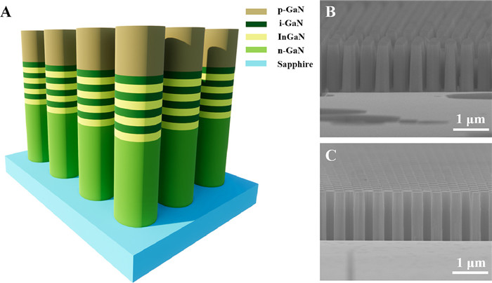
(A) Schematic of GaN NWs grown on sapphire substrate, SEM images of GaN NWs before (B) and after (C) surface treatment, respectively. Scale bar in (B) and (C) are 1 µm.
Surface treatment of GaN nanowires for enhanced photoelectrochemical water-splitting
Wenhao Chen , Jian Du , Hanbin Zhang , Hancheng Wang , Kaicheng Xu , Zhujun Gao , Jiaming Tong , Jin Wang , Junjun Xue , Ting Zhi , Longlu Wang

Solar energy and water are earth-abundant and sustainable sources for human beings. Facing the rising demand for energy, the utilization of photoelectrochemical (PEC) water splitting, which converts solar energy into hydrogen energy, is a promising approach to alleviate current energy issues [1–11]. Several individual enhancement strategies have been investigated to achieve high solar-to-hydrogen conversion (STH) efficiency, including plasmon enhancement [12–14], co-catalysts modification [15–18], nanostructures [10,19–22]. Among these approaches, nanostructured photoelectrode is a promising approach due to its advantages such as higher specific surface area, enhanced light absorption, and faster carrier separation [22–28]. In addition, the conduction band minimum (CBM) and valence band maximum (VBM) of GaN can span the redox potential of water, making Ⅲ-nitride nanostructure a promising candidate for PEC water splitting [27–35]. However, the presence of unavoidable surface states on GaN nanowires (NWs) acts as carrier recombination centers, inducing both surface Fermi level pinning and surface energy band bending [23–25,35–39]. Particularly, the naturally oxidized gallium oxide (GaOX) formed on the GaN NWs surface would act as a carrier trapping center, preventing the transfer of photogenerated holes from the NWs to the electrolyte. The presence of carrier traps on the NWs surface will introduce upward band bending, reducing the extraction probability of photogenerated carriers to the electrolyte and thus impair the PEC water splitting performance. It makes NWs subject to photo-corrosion with low chemical and structural stability, limiting the applications of NWs in PEC.
To overcome the effect of the surface states in PEC, many surface treatment methods have been investigated [21,28,35,38,40–53]. The Boon S Ooi group conducted a surface treatment on Pt-decorated GaN NWs photoelectrodes by organic thiol compounds. This method resulted in an enhanced photocurrent intensity of approximately −31 mA/cm2 at a potential of −0.2 V versus the reversible hydrogen electrode (vs. RHE) when using 1 mol/L H2SO4 as the electrolyte [40]. Son et al. fabricated a nano-porous GaN structure through hydrochloric acid (HCl) solution treatment for water splitting. Compared with the planar GaN, nano-porous GaN showed a four-fold enhancement, which can be attributed to the surface chemical bonds and band reconstruction [41]. One of the most popular surface treatment methods is wet etching using potassium hydroxide (KOH) alkaline solution to improve the surface quality of the photoelectrode by reducing defect density. Lee et al. studied the effect of KOH alkaline solution surface treatment on the formation of ohmic contact on p-type GaN (p-GaN). The contact resistivity decreased from 2.9 × 10⁻¹ Ω cm2 to 7.1 × 10⁻³ Ω cm2 after the surface treatment, indicating that KOH alkaline solution surface treatment can remove surface oxides effectively [42]. After comparing the results of p-GaN surface treatment with HCl solution and KOH solution, Sun et al. found that the surface Fermi level is closer to the valence band edge with a smaller surface barrier height after KOH alkaline solution surface treatment, leading to lower contact resistivity [43]. KOH alkaline solution can also effectively remove C and Cl contaminants from the Ga-polar surface and the oxides on the surface of Ga-polar GaN. However, the issue regarding the effect of alkaline solution surface treatment on p-n junction needs to be addressed without the use of extra co-catalysts and additional processes.
In this study, the performance of p-n GaN NWs was significantly enhanced by surface treatment using a 2 mol/L KOH alkaline solution, which reduced the presence of native oxides and dangling bonds on the surface. The GaN NWs sample after surface treatment (denoted as treated-NWs) exhibited an enhanced photocurrent (Jph) of approximately 10 µA/cm2 as well as a decreased leakage current, compared to the reference GaN NWs samples (denoted as untreated-NWs). Solid experimental evidence was provided by XPS fitting results, which demonstrated a reduction in oxide bonds on the GaN NWs surface after surface treatment. In addition, the time-resolved photoluminescence (TRPL) spectra showed a significant increase in carrier lifetime, indicating a reduction in non-radiative recombination centers. The results demonstrate the significance of optimized surface treatment, which can pave the way for the development of photoelectrodes in PEC water splitting.
A schematic diagram of the as-grown GaN-based photoanode is shown in Fig. 1A. The GaN NWs grown on sapphire substrate by metal organic chemical vapor deposition (MOCVD). The photoanode is composed of layers arranged from bottom to top, including a 2.5 µm thick Si-doped n-type GaN layer, a 200 nm thick GaN/InGaN multiple quantum wells (MQWs) absorption layer and a 400 nm thick Mg-doped p-type GaN layer. The MQWs consist of 15 periods of InGaN/GaN as a light absorbing layer. The indium incorporation in the wells was set to be approximately 0.2. The GaN-based epi‑wafers were cleaned by ultrasonic cleaning with acetone, ethanol, and deionized water for 10 min to remove the grease and impurities on the surface. Afterwards, the GaN NWs were fabricated using the soft ultraviolet (UV) curing nanoimprint lithography (NRL) technique, followed by inductively coupled plasma (ICP) dry etching using a nickel mask. As shown in Fig. 1B, the length of the NWs was controlled to approximately 1.3 µm for the exposed n-GaN region, the radius and period of the NWs were designed to be 300 and 600 nm, respectively. To minimize the surface damage and defects generated during the ICP etching process, surface treatments involving the utilization of hot potassium hydroxide (KOH) were conducted. The sample was immersed in a 2 mol/L KOH alkaline solution in water baths at a temperature of 60 ℃ for 4 min. Figs. 1B and C present scanning electron microscopy (SEM) images of the untreated-NWs and the treated-NWs photoanode samples, respectively. The images reveal a uniform cylindrical shape with nearly vertical and smooth sidewalls after the alkaline solution surface treatment. The smooth sidewalls contribute to the reduction of recombination centers and resistance to surface corrosion.
To demonstrate the removal of chemisorbed molecules and the passivation of dangling bonds on the GaN NWs surface by KOH alkaline solution treatment, the PEC characteristics of both the untreated-NWs and the treated-NWs were measured under incident light with a wavelength of 428 nm and a power of 1 mW/cm2. The results are shown in Figs. 2A–D. An electrochemical cell with a three-electrode system was used to investigate the PEC water splitting performance. The saturated Ag/AgCl and Pt mesh electrode were used as the reference and counter electrode, respectively. The conversion of potential from Ag/AgCl to RHE was computed using Eq. 1:
|
|
(1) |
in which EAg/AgCl0 = 0.197 V. In all of the PEC water splitting experiments, deionized water with a resistivity greater than 18.25 MΩ·cm was used as the electrolyte, with a pH value of approximately 7. The photogenerated electron-hole pairs are generated in the MQWs by absorbed incident light and then separated into the n-GaN and p-GaN by a built-in electric field of the p-n junction. Under the positive bias (defined by the current direction from the counter electrode to the NWs sample), the photogenerated electrons drift to the counter electrode through the external circuit and undergo redox reactions: 2H2O + 2e−= 2OH−+ H2. Meanwhile, the photogenerated holes move to p-GaN surface and participate in the reaction: 4OH−+ 4h+= O2 + 2H2O. Finally, the photocurrent can be collected by the electrochemical workstation while the OH− ions transport through the electrolyte to complete the current circuit. The photocurrents of GaN-based PEC under different external bias potentials were measured to estimate the redox performance of the samples. Here, the net photocurrent density (Jph) is defined as Jph = Jlight–Jdark, where Jlight and Jdark are the current density under illumination and in the dark, respectively. As shown in Figs. 2A–D, under the applied bias potentials of 0, 0.2, 0.4, and 0.6 V, the net photocurrent Jph of the treated-NWs increased from approximately 0.5, 0.6, 1.3, and 2.1 µA/cm² (for the untreated-NWs) to approximately 5.3, 5.8, 8.0, and 11.1 µA/cm², respectively. It is worth noting that the GaN-based PEC can operate without external bias, demonstrating the potential for self-driven device operation.

As shown in Fig. 3A, the photocurrent of the NWs samples was measured by linear sweep voltammetry (LSV) under illuminated conditions, with respect to the applied bias potentials ranging from approximately −0.2~2.6 V vs. RHE. The photocurrent density was increased after surface treatment, indicating improved carrier collection at the counter electrode. Furthermore, with further increase in the applied bias potential, a significant increase in photocurrent density can be observed in the treated-NWs samples, reaching approximately 10 µA/cm2. This clearly demonstrates the enhancement of PEC water splitting performance in the treated-NWs samples due to the surface treatment. As shown in Fig. 3B, electrochemical impedance spectroscopy (EIS) measurements were performed on both the untreated-NWs and the treated-NWs. It is widely accepted that the diameter of the Nyquist plot is a vital value of the interface charge transfer resistance (Rct) between the electrode and electrolyte [10,44]. Apparently, the diameter of the treated-NWs sample is smaller than that of the untreated-NWs, indicating a significant reduction in Rct due to surface treatment, which facilitates carrier transport. Moreover, the Nyquist plots were fitted using an equivalent circuit to investigate the change of Rct (the inset of Fig. 3B), consisting of electrolyte resistance (RΩ), electrochemical double layer capacitance (Cdl), Warburg impedance (ZW) and Rct.

To understand the dominant mechanism of surface treatment, the photoemission properties of the untreated-NWs and the treated-NWs samples were investigated and are shown in Fig. 4A. The room-temperature photoluminescence (PL) spectra of the untreated-NWs and the treated-NWs samples show the band edge position at 464.9 and 465.6 nm, respectively. The band edge emission intensity of the treated-NWs is five times stronger than that of the untreated-NWs. Additionally, there are no significant changes in the full-width at half maximum (FWHM) of the spectra. This observation can be attributed to the passivation of nonradiative recombination centers, the presence of which would otherwise capture photogenerated carriers and thus limit the PEC water splitting performance.
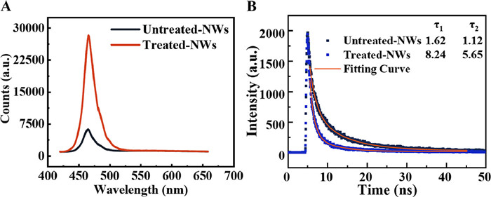
In addition, ultrafast laser spectroscopy was employed to analyze the dynamics of photoexcited electron in the treated-NWs. Fig. 4B illustrates the normalized time-resolved photoluminescence (TRPL) spectra around the band edge position (465 nm) for the untreated-NWs and the treated-NWs samples. A gradual decay curve, represented by the double exponential decay dashed line, fits well with the TRPL spectra. The fast and slow decay time constants (τ1 and τ2) of the untreated-NWs are estimated to be 1.62 and 1.12 ns, respectively, while those of the treated-NWs are 8.24 and 5.65 ns. The nonradiative recombination lifetime in the GaN material is significantly shorter compared to the radiative recombination lifetime. The observed slower decay of the treated-NWs compared to the untreated-NWs provides solid evidence that surface states can be effectively removed by alkaline solution surface treatment, thus resulting in increased Jph, improved Von, and increased PEC water splitting efficiency [40].
To investigate the changes in the chemical properties of GaN NWs following surface treatment with an alkaline solution, X-ray photoelectron spectroscopy (XPS) analysis was performed. Figs. 5A and B showed the XPS scans of N 1s, Ga 3d of the untreated-NWs and the treated-NWs, respectively. As shown in Fig. 5B, when the KOH alkaline solution etch was carried out, the peak for Ga 3d shifted to lower binding energy, related to a reduction in GaOx at the surface. A similar peak shift was also observed for the Ga 2p peak after treatment. The N 1s spectrum consists of the N signal from GaN and the Ga Auger signal at the lower energy side. To further investigate the effect of treatment on the NWs surface, the XPS peaks of Ga 2p and O 1s were analyzed in detail.

In Fig. 5C, the XPS spectra of Ga 2p3/2 can be decomposed into three peaks with peak positions of 1117 ± 0.1 eV (peak A), 1117.6 ± 0.15 eV (peak B) and 1118.1 ± 0.1 eV (peak C), corresponding to Ga-N bond, Ga-OH species and O-Ga-OH species, respectively. The shift of Ga 2p3/2 peak can be attributed to the increased peak intensity of the Ga-OH species and O-Ga-OH species. After the hydroxyl groups attach to the GaN surface, the surrounding Ga atoms are partially oxidized instead of forming random oxides. The Ga-O/Ga-N ratio is equal to the ratio of oxygen to nitrogen on the surface (O/N), which is improved after surface treatment.
To demonstrate the effectiveness of surface treatment in removing surface oxides and dangling bonds, we performed a split-peak fitting analysis of the O 1s core level energy spectra of the untreated-NWs and the treated-GaN NWs samples (Fig. 5D). The peaks corresponding to O-Ga in the O 1s spectra of GaN NWs after the alkaline solution surface treatment are significantly reduced, which indicates that gallium oxide can be effectively removed by the alkaline solution. The O 1s core level spectra can be decomposed into three peaks with peak positions of 531.2 ± 0.1 eV (peak Ⅰ), 532.0 ± 0.15 eV (peak Ⅱ) and 532.6 ± 0.15 eV (peak Ⅲ), corresponding to the O2− bonded state, oxygen in the hydroxyl group and O=C bonded state on the GaN surface. Comparing the hydroxyl peaks of the untreated-NWs and the treated-NWs, the proportion of hydroxyl groups increases significantly after surface treatment. In addition, the oxygen in the O=C bonded state is significantly reduced as well. It proves that the carbon on GaN surface can be effectively removed by the alkaline solution.
To further study the influences of the KOH alkaline solution treatment on the electronic structure of the NWs, theoretical investigations based on density functional theory (DFT) calculations were carried out. As shown in Figs. 6A–C, three models were considered, where an oxygen atom substitutes different positions of nitrogen atoms on GaN(11–20) surface (Figs. 6A and B), and a hydroxyl group is adsorbed on GaN(11–20) surface (Fig. 6C). These models are denoted as GaN(11–20): Ga-O(Ⅰ), GaN(11–20): Ga-O(Ⅱ), and GaN(11–20): Ga-OH, respectively. Based on these three models, the density of states (DOS) calculations were conducted to study the electronic structures (Figs. 6D–F). As shown in Figs. 6D and E, the presence of Ga-O bonds on the NWs surface causes the Fermi level to shift upward into the conduction band, resulting in the NWs surface exhibiting a metallic-like property. This property can be simply understood as n-type doping, where the O atom has one more electron than the N atom it replaces. From the DOS plots, it can be inferred that there is a downward band bending, which hinders the migration of holes from the NWs surface to the electrolyte. However, as shown in Fig. 6F, after the surface treatment with alkaline solution, the Ga-O bonds on the surface break and form Ga-OH bonds. This leads to the downward shift of the surface Fermi level, which indicates a upward band bending and a unpinned surface Fermi level. This is beneficial for the migration of photogenerated holes to the electrolyte, enhancing the charge carrier separation and ultimately improving the PEC performance of the NWs.

In summary, we have demonstrated a significantly enhancement in the PEC performance of the GaN NWs photoanodes by surface treatment. Compared with the GaN NWs reference sample, the GaN NWs with alkaline solution surface passivation show enhanced Jph, reaching a maximum of approximately 10 µA/cm2. The enhancement is mainly attributed to the following factors: (ⅰ) improved separation of charge carriers by optimizing flat band and band edge potential; and (ⅱ) enhanced carrier lifetime by suppressing -O bonds on the NWs surface. It has been proven that surface treatment is a vital step toward an improved photoelectrode for PEC water splitting applications.
The authors declare that they have no known competing financial interests or personal relationships that could have appeared to influence the work reported in this paper.
This work was funded by the National Key R&D Program of China (No. 2021YFB3601600), Innovation Support Programme (Soft Science Research) Project Achievements of Jiangsu Province (No. BK20231514), the National Nature Science Foundation of China (Nos. 61974062, 62004104), the Leading-edge Technology Program of Jiangsu Natural Science Foundation (No. BE2021008–2), and The Fundamental Research Foundation for the Central Universities, Collaborative Innovation Center of Solid-State Lighting and Energy-Saving Electronics.
Supplementary material associated with this article can be found, in the online version, at doi:
K. Ohashi, J. McCann, J.O.M.J.N. Bockris, Nature 266 (1977) 610–611. doi: 10.1038/266610a0
M. Gratzel, Nature 414 (2001) 338–344. doi: 10.1038/35104607
M. Gratzel, Nature 421 (2003) 586–587. doi: 10.1038/421586a
X. Chen, S. Shen, L. Guo, S.S. Mao, Chem. Rev. 110 (2010) 6503–6570. doi: 10.1021/cr1001645
M.G. Walter, E.L. Warren, J.R. McKone, et al., Chem. Rev. 110 (2010) 6446–6473. doi: 10.1021/cr1002326
H.M. Chen, C.K. Chen, R.S. Liu, et al., Chem. Soc. Rev. 41 (2012) 5654–5671. doi: 10.1039/c2cs35019j
S.D. Tilley, M. Grätzel, Energy Procedia 22 (2012) 1–2. doi: 10.1016/j.egypro.2012.05.230
T. Wang, J. Gong, Angew. Chem. Int. Ed. 54 (2015) 10718–10732. doi: 10.1002/anie.201503346
D. Cao, B. Wang, X. Yan, et al., Cryst. Growth Des. 23 (2023) 1530–1537. doi: 10.1021/acs.cgd.2c01117
C. Ramesh, P. Tyagi, V. Aggarwal, et al., ACS Appl. Nano Mater. 6 (2023) 1898–1909. doi: 10.1021/acsanm.2c04864
A. Abdullah, A. Waseem, I.V. Bagal, et al., ACS Appl. Nano Mater. 6 (2023) 1395–1404. doi: 10.1021/acsanm.2c05021
Z. Liu, D. Jiang, L. Yang, et al., Nano Energy 88 (2021) 106302. doi: 10.1016/j.nanoen.2021.106302
F. Tong, X. Liang, M. Liu, et al., ACS Catal. 12 (2022) 3558–3565. doi: 10.1021/acscatal.2c00486
J. Zhang, A. Reda Woldu, X. Zhao, et al., Appl. Surf. Sci. 598 (2022) 153745. doi: 10.1016/j.apsusc.2022.153745
M. Liu, Y. Chen, J. Su, et al., Nat. Energy 1 (2016) 16151. doi: 10.1038/nenergy.2016.151
L. Cheng, Q. Chen, J. Li, H. Liu, Appl. Catal. B 267 (2020) 118379. doi: 10.1016/j.apcatb.2019.118379
Z.X. Bi, R.T. Guo, X.Y. Ji, et al., Int. J. Hydrogen Energy 47 (2022) 34430–34443. doi: 10.1016/j.ijhydene.2022.08.028
S. Jayachitra, D. Mahendiran, P. Ravi, et al., Appl. Catal. B 307 (2022) 121159. doi: 10.1016/j.apcatb.2022.121159
B. AlOtaibi, M. Harati, S. Fan, et al., Nanotechnology 24 (2013) 175401. doi: 10.1088/0957-4484/24/17/175401
J. Benton, J. Bai, T. Wang, Appl. Phys. Lett. 102 (2013) 173905. doi: 10.1063/1.4803926
H. Son, P. Uthirakumar, T.H. Chung, et al., Appl. Surf. Sci. 547 (2021) 149105. doi: 10.1016/j.apsusc.2021.149105
H. Zheng, C. Zhao, S. Hu, et al., Phys. Status Solidi A 220 (2023) 2300037. doi: 10.1002/pssa.202300037
M.W. Chen, J.R.D. Retamal, C.Y. Chen, J.H. He, IEEE Electron Device Lett. 33 (2012) 411–413. doi: 10.1109/LED.2011.2180012
H.P. Wang, T.Y. Lin, C.W. Hsu, et al., ACS Nano 7 (2013) 9325–9335. doi: 10.1021/nn404015y
J.R.D. Retamal, C.Y. Chen, D.H. Lien, et al., ACS Photonics 1 (2014) 354–359. doi: 10.1021/ph4001108
D.H. Lien, J.R. Retamal, J.J. Ke, et al., Nanoscale 7 (2015) 19874–19884. doi: 10.1039/C5NR06494E
S. Noh, J. Shin, Y.T. Yu, et al., Nanomaterials 13 (2023) 358 (Basel).
A. Abdullah, I.V. Bagal, A. Waseem, et al., Mater. Today Phys. 28 (2022) 100846. doi: 10.1016/j.mtphys.2022.100846
B. AlOtaibi, H.P. Nguyen, S. Zhao, et al., Nano Lett. 13 (2013) 4356–4361. doi: 10.1021/nl402156e
M.G. Kibria, H.P. Nguyen, K. Cui, et al., ACS Nano 7 (2013) 7886–7893. doi: 10.1021/nn4028823
B. AlOtaibi, S. Fan, S. Vanka, et al., Nano Lett. 15 (2015) 6821–6828. doi: 10.1021/acs.nanolett.5b02671
S. Fan, B. AlOtaibi, S.Y. Woo, et al., Nano Lett. 15 (2015) 2721–2726. doi: 10.1021/acs.nanolett.5b00535
Y. Wang, B. AlOtaibi, F.A. Chowdhury, et al., APL Mater. 3 (2015) 116106. doi: 10.1063/1.4935307
A. Abdullah, A. Waseem, I.V. Bagal, et al., ACS Appl. Energy Mater. 4 (2021) 13759–13765. doi: 10.1021/acsaem.1c02486
D. Wang, W. Wu, S. Fang, et al., Light Sci. Appl. 11 (2022) 227. doi: 10.1038/s41377-022-00912-7
C.Y. Chen, J.R.D. Retamal, I.W. Wu, et al., ACS Nano 6 (2012) 9366–9372. doi: 10.1021/nn205097e
M. Sato, Y. Imazeki, T. Takeda, et al., J. Phys. Chem. C 125 (2021) 25807–25815. doi: 10.1021/acs.jpcc.1c07110
N. Kumar, A. Kumar, F. Chand, Appl. Phys. Lett. 122 (2023) 013503. doi: 10.1063/5.0134242
Y. Xiao, S. Vanka, T.A. Pham, et al., Nano Lett. 22 (2022) 2236–2243. doi: 10.1021/acs.nanolett.1c04220
P. Varadhan, H.C. Fu, D. Priante, et al., Nano Lett. 17 (2017) 1520–1528. doi: 10.1021/acs.nanolett.6b04559
H. Son, J.H. Park, P. Uthirakumar, et al., Appl. Surf. Sci. 532 (2020) 147465. doi: 10.1016/j.apsusc.2020.147465
J.L. Lee, J.K. Kim, J.W. Lee, et al., Solid State Electron. 43 (1999) 435–438. doi: 10.1016/S0038-1101(98)00265-2
J. Sun, K.A. Rickert, J.M. Redwing, et al., Appl. Phys. Lett. 76 (2000) 415–417. doi: 10.1063/1.125772
S. Deng, D. Sun, C. Wu, et al., Electrochim. Acta 111 (2013) 707–712. doi: 10.1016/j.electacta.2013.08.055
K. Deng, X. Wang, S. Huang, et al., ACS Appl. Mater. Interfaces 15 (2023) 25058–25065. doi: 10.1021/acsami.3c03094
X.D. Wang, Y.H. Huang, J.F. Liao, et al., Nat. Commun. 12 (2021) 1202. doi: 10.1038/s41467-021-21487-8
Z. Xu, S. Zhang, J. Liang, et al., J. Power Sources 419 (2019) 65–71. doi: 10.1016/j.jpowsour.2019.02.050
M. Reddeppa, B.G. Park, S. Majumder, et al., Nanotechnology 31 (2020) 475201. doi: 10.1088/1361-6528/aba301
Q. Yu, M. Yang, X. Luo, et al., Appl. Phys. Lett. 119 (2021) 013903. doi: 10.1063/5.0047079
M.A. Hassan, J.H. Kang, M.A. Johar, et al., Acta Mater. 146 (2018) 171–175. doi: 10.1016/j.actamat.2017.12.063
C. Wang, S. Wei, F. Li, et al., Nanoscale 12 (2020) 3259–3266. doi: 10.1039/c9nr09502k
X. Wan, Y. Xu, X. Wang, et al., Appl. Surf. Sci. 573 (2022) 151492. doi: 10.1016/j.apsusc.2021.151492
H.M. Li, Z.Y. Wang, H.J. Jing, et al., Appl. Catal. B 284 (2021) 119760. doi: 10.1016/j.apcatb.2020.119760

Figure 1 (A) Schematic of GaN NWs grown on sapphire substrate, SEM images of GaN NWs before (B) and after (C) surface treatment, respectively. Scale bar in (B) and (C) are 1 µm.

Figure 2 I-t curves of the untreated-NWs (blue curve) and the treated-NWs (red curve) under the incident light with wavelength of 428 nm and power of 1 mW/cm2 driven by the external bias voltage of (A) 0 V, (B) 0.2 V, (C) 0.4 V, (D) 0.6 V.

Figure 3 (A) LSV images of the untreated-NWs (black curve) and the treated-NWs (red curve) with the vertical axis representing the current density of net current Jph under 1 mW/cm2 illumination with wavelength of 428 nm in the deionized water (pH 7). (B) EIS measurements of the untreated-NWs (black dots) and the treated-NWs (blue dots), the red curves represent the fitting curve.

Figure 4 (A) Room-temperature PL spectra of the untreated-NWs (black curve) and the treated-NWs (red curve). (B) TRPL carrier lifetime of the untreated-NWs (black dots) and the treated-NWs (blue dots), where the fast and slow decay time constants (τ1 and τ2) are shown in the figure.

Figure 5 XPS spectra of (A) N 1s, (B) Ga 3d, (C) Ga 2p3/2 and (D) O 1s scans for untreated-NWs and treated-NWs. Among them, Ga 2p3/2 spectra of the untreated-NWs and the treated-NWs, which can be divided into three peaks A, B, and C, corresponding to Ga-N bond, Ga-OH species, and O-Ga-OH species, respectively. (D) O 1s can be divided into three peaks Ⅰ, Ⅱ, and Ⅲ, corresponding to O2− bonding state, oxygen in hydroxyl group, and O=C bonding state.

 扫一扫看文章

扫一扫关注我们
 DownLoad:
 下载:
下载:

 下载:
下载: