Citation:
Kaiming Yang, Min Lv, Yanhong Chang, Kun Lu, Zhixiang Wei. Oligomeric donor with appropriate crystallinity for organic solar cells[J]. Chinese Chemical Letters,
2024, 35(2): 109018.
doi:
10.1016/j.cclet.2023.109018
Oligomeric donor with appropriate crystallinity for organic solar cells
English
Oligomeric donor with appropriate crystallinity for organic solar cells
CAS Key Laboratory of Nanosystem and Hierarchical Fabrication, CAS Center for Excellence in Nanoscience, National Center for Nanoscience and Technology, Beijing 100190, China
b.
University of Chinese Academy of Sciences, Beijing 100049, China
c.
Department of Environmental Science and Engineering, University of Science and Technology Beijing, Beijing 100083, China
d.
Beijing Key Laboratory of Resource Treatment of Typical Industrial Pollutants, Beijing 100083, China
lvk@nanoctr.cn (K. Lu). 1 These authors contributed equally to this work.
Received Date:
24 May 2023 Accepted Date:
30 August 2023 Revised Date:
29 August 2023 Available Online:
15 February 2024
Abstract:
Improving the performance of all-small-molecule organic solar cells (ASM-OSCs) largely depends on the design and application of novel donors with appropriate crystallinity. Extending molecular conjugation is an effective method for regulating molecular stacking and crystallinity. In this work, we successfully designed and synthesized two novel acceptor-donor-donor-donor-acceptor (A-D-D-D-A) type oligomeric donors with three dithieno[2,3-d:2’,3’-d’]benzo[1,2-b:4,5-b’]dithiophene (DTBDT) as the central unit, named as 3DTBDT-Cl and 3DTBDT, depending on with and without chlorine substitution on the thiophene side chains. We found that the introduction of chlorine atoms makes the blend films display stronger crystallinity but with large-scale phase separation morphology and more defects, which eventually leads to a power conversion efficiency (PCE) of only 10.83%, whereas the blend films based 3DTBDT with appropriate crystallinity achieved 13.74% PCE. Compared with 3DTBDT-Cl/L8-BO, the 3DTBDT/L8-BO films exhibited a nanoscale bi-continuous interpenetrating network morphology with a smaller domain size and more suitable crystallinity, which guarantees the corresponding devices obtained more efficient exciton dissociation, efficient charge transport, reduced bimolecular recombination, and performed more balanced carrier mobility. These results demonstrated that regulating the crystallinity of oligomeric donors to obtain the desired phase separation morphology in the blend films could facilitate further improving the performance of ASM-OSCs.
Solution-processed bulk heterojunction (BHJ) organic solar cells (OSCs) have become research frontiers in recent decades because of their unique advantages, such as low cost, flexibility and solution processability [1–8]. Thanks to the synthesis of new photovoltaic materials and optimization of device processes, especially the development and application of new Y series non-fullerene small molecule acceptors [9–14], the PCE of single junction polymer organic solar cells (PSCs) have exceeded 19% [15–18]. However, while polymeric donors have high efficiency and outstanding process film-forming, batch-to-batch production issues potentially limit their industrial applications. Compared with polymers, small or oligomeric donors can resolve these problems in the production process more effectively duo to their definite molecular structure [19,20]. In recent years, the PCE of all-small-molecule organic solar cells (ASM-OSCs) have also achieved more than 17% [21,22], but their performance still lags behind that of PSCs. This is mainly due to the short and similar molecular structures of A-π-D-π-A type donors and acceptors, which have similar physical and chemical properties, making it difficult to regulate the crystallinity of donor and acceptor materials, and it is not easy to form a blend film morphology of nanoscale interpenetrating network structures, resulting in relatively low short circuit current (JSC) and fill factor (FF).
The regulation of nanomorphology is highly dependent on the crystallinity of the molecule itself and the compatibility of small molecule donors (SMDs) and acceptors. Broadening the conjugation of the molecular plane is a common and effective method to regulate the crystallinity of donors. Li et al. designed and synthesized two A-π-D-π-A type small donors H11 and H12, with and without thiophene conjugated side chains on the benzo[1,2-b:4,5-b’]dithiophene (BDT) unit, respectively [23]. Compared to the H12, the 2D-conjugated H11 with thiophene conjugated side chains shows intense absorption, low-lying HOMO energy level, higher hole mobility and ordered bimodal crystallite packing in the blend films, which leads to the corresponding devices achieve a higher PCE of 9.73%. Hou et al. synthesized an A-π-D-π-A type SMD (named as B1) based on phenyl-substituted BDT central unit, which improved crystalline properties and increased intermolecular π-π interaction, in comparison with those of its corresponding thiophene-substitute BDT-based counterpart [24]. After the effective modulation of the active layer morphology, charge separation and transport efficiencies were greatly improved, and ASM-OSCs achieved a higher PCE of 15.3%.
Expanding the fused rings of central core can also enhance crystallinity [25,26]. To our knowledge, dithieno[2,3-d:2′,3′-d’]benzo[1,2-b:4,5-b’]dithiophene (DTBDT) unit holds an extended conjugation length, therefore a stronger electron donating ability and carrier mobility, making it a highly desirable small molecule donor unit in donors. In recent years, a series of DTBDT-based SMDs have been synthesized, resulting in continuous enhancements of the efficiency of ASM-OSCs [27–30]. In particular, we synthesized a series of SMDs ZR1, ZR1-Cl, and ZR1-S-Cl based on DTBDT in 2020 [27]. By introducing chlorine and sulfur chlorine atoms to improve the crystallinity of SMDs further, a bi-continuous interpenetrating network was formed in the ZR1-S-Cl/IDIC-4Cl blend films, achieving the highest PCE of 12.05%. On this basis, developing novel oligomeric donors with more suitable crystallinity and a longer conjugated backbone is expected to be an effective strategy for realizing high-performance ASM-OSCs.
Based on the SMDs ZR1-Cl, we designed and synthesized a novel linked-DTBDT type oligomeric donor 3DTBDT-Cl using a DTBDT unit with a larger conjugation plane instead of the original double thiophene π-bridge in ZR1-Cl (Fig. 1a). The 3DTBDT-Cl/L8-BO based devices only yielded a low PCE of 10.83% due to excessive phase separation of the blend films caused by the undue crystallinity of 3DTBDT-Cl. Therefore, the oligomeric donor 3DTBDT was synthesized to reduce the crystallinity by removing the chlorine atoms later. As we expected, the removal of chlorine atoms successfully endowed the oligomeric 3DTBDT with appropriate crystallinity. After blending with L8-BO, high-quality films were obtained with smoother surface, appropriate crystallinity, and more uniform nanofiber phase separation structure. Therefore, the devices showed more effective exciton dissociation and charge collection, higher carrier mobility, longer charge lifetime, and effective inhibition of bimolecular recombination. As a result, the optimized 3DTBDT/L8-BO-based devices obtained a higher FF of 70.98%, JSC of 22.84 mA/cm2, and PCE of 13.74%. The results indicated that the blend films with appropriate crystallinity and phase separation could be achieved by slightly changing the structures of the oligomeric donors, thereby achieving higher photovoltaic performance in ASM-OSCs.
Figure 1
Figure 1.
(a) Molecular structures of SMDs ZR1-Cl, oligomeric donors 3DTBDT-Cl and 3DTBDT, and small molecule acceptor L8-BO. (b, c) Normalized UV–vis absorption spectra of 3DTBDT-Cl, 3DTBDT, L8-BO in solution and thin films. (d) Energy diagrams of 3DTBDT-Cl, 3DTBDT, L8-BO.
The synthetic routes of the oligomeric donors 3DTBDT-Cl and 3DTBDT are presented in Scheme S1 (Supporting information). And the detailed synthesis methods, 1H nuclear magnetic resonance (1H NMR) and matrix-assisted laser desorption/ionization time of flight mass spectrometry (MALDI-TOF MS) analysis were clearly provided in Supporting information. The optical absorption properties of 3DTBDT-Cl and 3DTBDT were investigated using an ultraviolet-visible (UV–vis) spectrophotometer. In the chloroform solution state, the absorption of 3DTBDT was broader than that of 3DTBDT-Cl, but there was no significant shoulder peak, which means that the two donors did not form the pre-aggregated state (Fig. 1b). In the thin film state, both donors performed significantly red-shifted and strong shoulder peaks, indicating that both donors achieved strong intermolecular interaction in the films (Fig. 1c). Likewise, we found that the absorption edges of 3DTBDT-Cl and 3DTBDT films were located at 620 nm and 633 nm, corresponding to the optical bandgap of 1.93 eV and 1.74 eV, respectively. In summary, 3DTBDT showed a broader absorption spectrum and narrower optical bandgap in the film state, and effectively provides complementary absorption for L8-BO, which is beneficial to achieve high JSC in devices.
The highest occupied molecular orbital (HOMO) and the lowest unoccupied molecular orbital (LUMO) of the oligomeric donors 3DTBDT-Cl, 3DTBDT and acceptor L8-BO in the films were determined by cyclic voltammetry (CV) measurements with Ag/Ag+ as the reference electrode (Fig. S3 in Supporting information). Based on the equation EHOMO/LUMO = −(Eox/red − EFc/Fc1/2 + 4.8) eV, the HOMO/LUMO of the 3DTBDT-Cl, 3DTBDT and L8-BO were calculated to be ‒5.48/‒3.55, ‒5.33/‒3.59 and ‒5.67/‒3.92 eV (Fig. 1d) [31,32]. Apparently, the identical end-group in both donors provides similar LUMO energy levels, whereas introducing chlorine atoms weakens the electron-donating ability within the 3DTBDT-Cl, resulting in a lower HOMO energy level and a wider band gap, which is consistent with the UV–vis results. The lower HOMO energy level of 3DTBDT-Cl will help the 3DTBDT-Cl/L8-BO based devices to obtain higher VOC.
To investigate the device performance, we used L8-BO as the acceptor and fabricated OSCs using a conventional architecture of ITO/PEDOT: PSS/active layer/PDINO/Ag. The optimal preparation conditions for the active layer were determined by adjusting the concentration of the solution after mixing with the acceptor, the D/A ratio, the rotational speed of the film, the type of interfacial layer, and the thermal annealing temperature. The detailed optimization conditions and results are summarized in Tables S6-S9 (Supporting information). As shown in the current density-voltage (J-V) plots (Fig. 2a) and the summary of the detailed parameters (Table 1), the 3DTBDT-Cl/L8-BO based devices revealed a relatively low PCE of 10.83%, a JSC of 18.80 mA/cm2, an FF of 62.62% and a higher VOC of 0.920 V. However, the 3DTBDT/L8-BO devices exhibited significantly enhanced PCE of 13.74%, with a JSC of 22.84 mA/cm2, a FF of 70.98%, and a VOC of 0.847 V. Fig. 2b showed the external quantum efficiency (EQE) spectra of the two optimized systems, it can be seen that all the blends exhibited a broad absorption range from 300 nm to 930 nm, with the maximum value of 66.09% and 80.74% for 3DTBDT-Cl and 3DTBDT based devices, respectively. The error between JSC calculated from the EQE curve and the corresponding values measured from the J-V tests is within 5%, proving the reliability of the measured device performance.
Figure 2
Figure 2.
(a) Optimized J-V curves for conventional devices. (b) EQE corresponding to devices. (c) Transient photovoltage (TPV) curves of optimal devices. (d) Transient photocurrent (TPC) curves of optimal devices.
Whereafter, the difference in energy loss between 3DTBDT-Cl and 3DTBDT-based devices was investigated. According to the Shockley-Queisser (SQ) limit [33,34], they divided Eloss in OSCs into three parts: Eloss = qΔVOC = Eg – qVOC = ΔE1 + ΔE2 + ΔE3, where Eg is the photovoltaic energy bandgap extracted from the derivation of the EQEPV curve. ΔE1 is originated from the radiative recombination above the band gap, which is unavoidable for any type of solar cell, so the ΔE1 value (0.265 eV) is almost the same for the two devices. ΔE2 is due to the extra radiative recombination below the band gap and OSCs have a large loss of this fraction due to the presence of CT states, which can be reduced by raising the CT state [35–37]. The ECT can estimate from normalized fourier-transform photocurrent spectroscopy external quantum efficiency (FTPS-EQE) curves and electroluminescence (EL) spectra of devices (Fig. S5 in Supporting information). As shown in Table S2 (Supporting information), the ΔECT (Eg – ECT) for 3DTBDT-Cl/L8-BO (0.016 eV) is significantly lower than 3DTBDT/L8-BO (0.042 eV), which indicates a lower ΔE2 value for 3DTBDT-Cl/L8-BO (0.089 eV), whereas a high ΔE2 for 3DTBDT/L8-BO (0.112 eV) systems. ΔE3 (ΔE3 = [–kT/q ln (EQEEL)]) is observed due to nonradiative recombination, where k is the Boltzmann constant, T is the Kelvin temperature, EQEEL is the electroluminescence in the dark state, and the luminescence efficiency of the device is directly related to the nonradiative recombination [38]. The EQEEL of the two devices are shown in Fig. S6 (Supporting information), compared with 3DTBDT/L8-BO, 3DTBDT-Cl/L8-BO exhibited a higher EQEEL value of 1.18 × 10⁻³ and a smaller ΔE3 value of 0.174 eV, which can be explained lower ΔECT endowed a stronger coupling between singlet and CT states, indicating the nonradiative recombination loss was reduced in the corresponding system. The total voltage loss of the 3DTBDT-Cl based device is smaller at 0.528 V, which explains the higher VOC obtained for the corresponding device. However, the JSC and FF were limited by the unsuitable blend film morphology.
In order to gain more insight into the charge extraction/recombination dynamics of devices, we used transient photovoltage (TPV) and transient photocurrent (TPC) tests [39]. The carrier lifetimes can be extracted from fitting the TPV decay dynamics. We found that the carrier lifetime of 3DTBDT/L8-BO (27 µs) was much longer than that of 3DTBDT-Cl/L8-BO (10 µs) (Fig. 2c). The longer charge lifetime also implies less charge recombination. As shown in Fig. 2d, by fitting the transient TPC decay dynamics, the charge extraction time is found to be 38 ns for 3DTBDT/L8-BO and 40 ns for 3DTBDT-Cl/L8-BO system. The shorter charge extraction time of 3DTBDT-based devices is due to the higher carrier mobility and the excellent charge properties, which facilitated charge collection and ensured that the corresponding devices obtained higher FF and improved absorption photon utilization (JSC). These results were further validated by the exploration of molecular stacking and morphology.
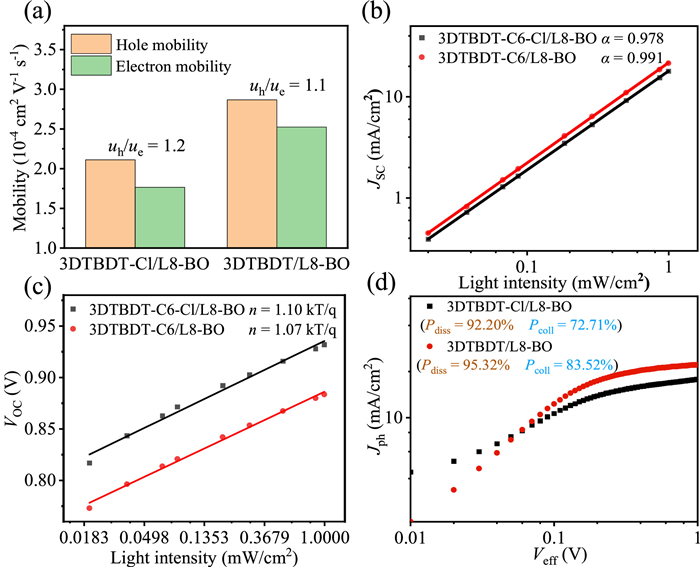
To investigate the effect of charge transport properties of the devices, we used the space-charge limited current (SCLC) method to measure the hole mobility (µh) and electron mobility (µe) of the blend films. As shown in Fig. 3a, the µh and µe of the 3DTBDT-Cl/L8-BO based device are 2.112 × 10⁻⁴ cm2 V−1 s–1 and 1.765 × 10⁻⁴ cm2 V−1 s–1, respectively, with a µh/µe ratio of 1.2. By contrast, 3DTBDT/L8-BO not only afforded increased hole and electron mobilities of 2.867 × 10⁻⁴ cm2 V−1 s–1 and 2.524 × 10⁻⁴ cm2 V−1 s–1, respectively, but also had a more balanced µh/µe ratio of 1.1, which indicates that the devices displayed a more balanced hole and electron transport capability. The increase of FF and JSC can attribute to the improvement of charge transport performance. The relatively low and unbalanced hole and electron mobility for 3DTBDT-Cl/L8-BO based device leads to more charge recombination, which results in lower FF and JSC.
Figure 3
Figure 3.
(a) Hole and electron mobility of optimized devices. (b) JSC and (c) VOCversus the natural logarithm of the light intensities of optimized devices. (d) Dependence of the photocurrent density (Jph) on the effective voltage (Veff).
The charge recombination mechanism can be explored by investigating the dependence of JSC and VOC on incident light intensity (Plight). The dependence of Jsc on Plight is defined by the equation JSC ∝ (Plight)α, α refers to the exponential factor, and the closer its value is to 1.0, the lower the probability of bimolecular recombination and the higher the charge collection efficiency [40]. The α values based on 3DTBDT-Cl/L8-BO and 3DTBDT/L8-BO based devices are 0.978 and 0.991, respectively, indicating that bimolecular recombination can be effectively suppressed in 3DTBDT/L8-BO blended film (Fig. 3b). The dependence of VOC on Plight is described by the equation VOC ∝ nkT/q ln(Plight), k is the Boltzmann constant, T is the absolute temperature, and q is the elementary charge [41]. The n values of 3DTBDT-Cl/L8-BO and 3DTBDT/L8-BO based devices are 1.07 and 1.10, respectively (Fig. 3c). This result indicated that the devices based on oligomeric donor 3DTBDT is beneficial to suppress the trap-assisted recombination and obtained higher JSC and FF.
To investigate the exciton dissociation and charge collection characteristics processes of the optimal devices, the relationship between the photocurrent density (Jph) and effective voltage (Veff) were characterized (Fig. 3d). Jph is defined as JL – JD, where JL and JD are the current densities under illumination and in the dark, respectively. Veff = V0 – Vapp, where V0 is the voltage when the Jph = 0 and Vapp represents the applied voltage bias [42]. When Veff reaches 2 V, it is assumed that the excitons are completely dissociated into free charge carriers and collected by the electrode at this high voltage to obtain a saturated current density (Jsat). The exciton dissociation probability (Pdiss) and charge collection efficiency (Pcoll) are calculated by the Jph/Jsat values under short-circuit and maximum power output conditions, respectively (Fig. 3d). Compared with the 3DTBDT-Cl/L8-BO based devices (Pdiss of 92.20% and Pcoll of 72.71%), 3DTBDT/L8-BO based device displayed much higher Pdiss (95.32%) and Pcoll (83.52%). The significant increase in Pdiss and Pcoll based on 3DTBDT/L8-BO is attributed to its lower µe/µh ratio, higher and more balanced hole and electron transport capacity, and better nanoscale bi-continuous interpenetrating network morphology.
Grazing incidence wide-angle X-ray scattering (GIWAXs) was used to reveal the crystallinity and stacking pattern of the pure and blend films. The 2D scattering patterns and corresponding cutline profiles in the in-plane (IP) and out-of-plane (OOP) directions are shown in Figs. 4a-f. From the diffraction patterns of two pure films, we can clearly see that both 3DTBDT-Cl and 3DTBDT exhibit the π-π (010) diffraction peaks in the IP direction and lamella stacking (100), (200), and (010) peaks in the OOP direction, indicating that they have molecular stacking patterns with edge-on and face-on mode. The Scheller equation was used to calculate the crystal coherence length (CCL), and the average size of the crystallites was studied. The CCL of 3DTBDT-Cl in the pure film was 25.10 Å, while that of 3DTBDT was 21.33 Å, these findings demonstrate that 3DTBDT-Cl is slightly more crystalline in nature than 3DTBDT. After blending with L8-BO, both blend films exhibited a strong (010) diffraction peak in the OOP direction, as well as a significantly weakened (100) peak and a disappeared (200) peak. Therefore, both systems showed a clear and strong face-on dominant orientation induced by the L8-BO, which facilitates the charge transport in OSCs towards the electrodes. Compared with 3DTBDT-Cl/L8-BO films (d = 3.81 Å, CCL = 18.91 Å), 3DTBDT/L8-BO films in the OOP direction showed a shorter CCL (d = 3.67 Å, CCL = 12.48 Å), which indicated that the 3DTBDT/L8-BO films can obtain more suitable crystallinity.
Figure 4
Figure 4.
2D GIWAXs images of (a) 3DTBDT-Cl pure film, (b) 3DTBDT pure film, (c) 3DTBDT-Cl/L8-BO blend film, (d) 3DTBDT/L8-BO blend film, and (e) corresponding 1D curves for GIWAXs, (f) d-spacing and crystal coherence length (CCL) in π-π stacking direction. AFM height images of (g) 3DTBDT-Cl/L8-BO blend film and (i) 3DTBDT/L8-BO blend film. TEM images of (h) 3DTBDT-Cl/L8-BO blend film and (j) 3DTBDT/L8-BO blend film. All blend films are prepared under optimal conditions.
The surface tensions (γ) of the donor and acceptor can be obtained by measuring the contact angles (CAs) of droplets with different polarities on the corresponding film surfaces. Fig. S7 and Table S5 (Supporting information) showed the CAs of water and glycerol droplets on the surfaces of 3DTBDT-Cl, 3DTBDT and L8-BO pure films. Then using Young’s equation, the γ values of the three materials can be calculated as 15.17, 16.07 and 17.75 mN/m [43]. The results revealed that the surface tension of 3DTBDT with ordinary alkyl side chains is close to that of L8-BO. According to the Flory-Huggins theory, the interaction parameter (χ) between 3DTBDT and L8-BO was calculated to be only 0.04, indicating that they have significant compatibility [44]. The introduction of chlorine atoms reduced the surface tension of 3DTBDT-Cl and increased the χ value with the acceptor to 0.10. The reduced χ value indicated better compatibility between the donor and acceptor, providing a driving force for the morphology modulation of the D/A blend film.
Atomic force microscopy (AFM) and transmission electron microscopy (TEM) were used to investigate the effect of active layer morphology on device performance. The AFM height image (Figs. 4g and i) displayed the mean-square roughness (Rq) of the 3DTBDT-Cl/L8-BO film was 1.47 nm, which revealed the existence of excessive aggregation in the blend films due to the stronger stacking and crystallinity of the donors, while a smaller Rq of 0.85 nm was observed in the 3DTBDT/L8-BO film, indicating that the optimized 3DTBDT/L8-BO film exhibited a smoother surface, which is conducive to the formation of better contact between the film and the electrode, thus promoting charge extraction. The TEM images (Figs. 4 h and j) were consistent with the AFM. It can be seen that the 3DTBDT-Cl/L8-BO film showed large-scale phase separation and more defects while 3DTBDT/L8-BO film formed a suitable nano-scale bi-continuous interpenetrating network that can facilitate charge separation and carrier transport, directly related to the higher JSC and FF in their corresponding devices. Although the optimized 3DTBDT-Cl/L8-BO film has stronger crystallinity, there is no obvious fiber structure or suitable phase separation, which explains the lower JSC and FF values.
In summary, we designed and synthesized two linked-DTBDT type oligomeric donors 3DTBDT-Cl and 3DTBDT, with and without chlorine atoms on the thiophene side chains, respectively. Compared to 3DTBDT-Cl, pure and blend films of 3DTBDT exhibit more appropriate crystallinity. Due to the excessive aggregation of the donors in the blend film, the 3DTBDT-Cl/L8-BO based device with only 10.83% PCE, 18.80 mA/cm2JSC and 62.62% FF, while the 3DTBDT-based device obtained 13.74% PCE, 22.84 mA/cm2Jsc and 70.98% of FF. Compared to 3DTBDT-Cl/L8-BO blend films, the 3DTBDT/L8-BO blend films with nanofiber structure achieved a smoother surface, proper crystallinity, and more uniform phase separation, which provides more efficient exciton dissociation and collection, reduced bimolecular recombination and more balanced carrier mobility. Therefore, 3DTBDT/L8-BO achieved better FF, JSC, and PCE. These results suggest that obtaining appropriate crystallinity and phase separation morphology in blend film by regulating the crystallinity of oligomeric donors is an effective approach to achieving high-performance ASM-OSCs.
Declaration of competing interest
The authors declare that they have no known competing financial interests or personal relationships that could have appeared to influence the work reported in this paper.
Acknowledgments
We acknowledge financial support provided by the National Natural Science Foundation of China (No. 51973043), and the Chinese Academy of Sciences (No. GJHZ2092–019).
Supplementary materials
Supplementary material associated with this article can be found, in the online version, at doi:10.1016/j.cclet.2023.109018.
Figure 1
(a) Molecular structures of SMDs ZR1-Cl, oligomeric donors 3DTBDT-Cl and 3DTBDT, and small molecule acceptor L8-BO. (b, c) Normalized UV–vis absorption spectra of 3DTBDT-Cl, 3DTBDT, L8-BO in solution and thin films. (d) Energy diagrams of 3DTBDT-Cl, 3DTBDT, L8-BO.
Figure 3
(a) Hole and electron mobility of optimized devices. (b) JSC and (c) VOCversus the natural logarithm of the light intensities of optimized devices. (d) Dependence of the photocurrent density (Jph) on the effective voltage (Veff).
Figure 4
2D GIWAXs images of (a) 3DTBDT-Cl pure film, (b) 3DTBDT pure film, (c) 3DTBDT-Cl/L8-BO blend film, (d) 3DTBDT/L8-BO blend film, and (e) corresponding 1D curves for GIWAXs, (f) d-spacing and crystal coherence length (CCL) in π-π stacking direction. AFM height images of (g) 3DTBDT-Cl/L8-BO blend film and (i) 3DTBDT/L8-BO blend film. TEM images of (h) 3DTBDT-Cl/L8-BO blend film and (j) 3DTBDT/L8-BO blend film. All blend films are prepared under optimal conditions.


 DownLoad:


 下载:
下载:


 下载:
下载:
