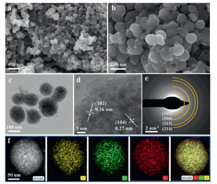
Figure 1.
(a, b) SEM images, (c) TEM image, (d) HRTEM image, (e) SAED pattern, (f) EDX elemental mapping of Od-V2O3@C materials.
Constructing oxygen-deficient V2O3@C nanospheres for high performance potassium ion batteries
Qiang Deng , Luolan Wang , Jing Li , Qian Cheng , Xiaozhao Liu , Changdong Chen , Qimeng Zhang , Wentao Zhong , Hua Wang , Lijue Wu , Chenghao Yang

In order to alleviate the energy crisis and utilize renewable energy, large scale energy storage system has received enormous attention, and it's urgent to develop a new type of low-cost energy storage device [1, 2]. Though commercial lithium-ion batteries (LIBs) have successfully dominated the market of portable products and electric vehicles, they have limited applications in the large scale energy storage system due to the uneven distribution and insufficient availability of lithium resources [3-5]. In this regard, potassium ion batteries (PIBs) hold the promise as complementary candidates to LIBs because of their abundant resource and low cost [6-9]. Furthermore, the low redox potential (−2.93 V vs. SHE) and weak Lewis acidity of K+ endow PIBs with high operating voltage and fast diffusion kinetics, respectively [10-12]. Nevertheless, the de/intercalation of large size of K+ (radius: 1.38 Å) is often accompanied by severe volume change, leading to unsatisfactory electrochemical performance, so it still remains great challenges to explore suitable electrode materials for high performance PIBs [13-15].
To date, a variety of anode materials have been exploited for PIBs, including carbon-base materials [16-18], alloy-type materials [19, 20], organic compounds [21, 22], and transition metal oxide/chalcogenides materials [23-26], etc. Among them, transition metal oxides have been intensively studied due to their high theoretical capacity and cost effectiveness [27]. As a representative, V2O3 with open tunnel structure of the 3D framework can achieve fast de/intercalation of K+, which has gain much interest in recent years [28, 29]. Unfortunately, it is difficult to realize high capacity and good rate capability owing to its low electronic conductivity [29, 30]. Besides, the large size of K+ will cause structure collapse during cycling, resulting in poor cycle life. To tackle these issues, the common strategy is morphology engineering and incorporating with carbon-based materials to construct composites [31]. For example, a self-standing V2O3@PNCNFs electrode reported by Jiao's group shows a reversible capacity of 240 mAh/g at 50 mA/g and maintains 95.8% capacity retention after 500 cycles [28]. In addition, deficiency engineering is also an efficient method to enhance electronic conductivity of the materials [32-34]. Li et al. [24] demonstrated that constructing oxygen-rich defect amorphous shell on VO2 surface can narrow the band gap of VO2, boosting K+ storage capability. To the best of our knowledge, there is little research combining the above strategies to develop PIBs with excellent cycling stability and rate capability.
Herein, oxygen-deficient V2O3 nanoparticles encapsulated in amorphous carbon shell (Od-V2O3@C) are rationally designed and synthesized by a facile solvothermal method followed by calcination and reduction process. The as-prepared Od-V2O3@C nanospheres are endowed with these following merits: (1) The nanostructure design guarantees the short diffusion distances and thus facilitates electron/K+ transfer. (2) The uniform amorphous carbon shell can enhance the electronic conductivity as well as maintain the structural stability. (3) The introduction of oxygen deficiency is capable of regulating the electronic structure of materials and greatly boosting the electrochemical performance. As a result, Od-V2O3@C electrode achieved superior rate capability and excellent long-term stability (127.4 mAh/g after 1000 cycles at 2 A/g). Such a synergistic strategy by combining morphology and deficiency engineering provides an effective way to exploit transition metal oxide with high performance for energy storage application.
Od-V2O3@C was prepared by solvothermal method followed by calcination and reduction process [35]. Firstly, a homogeneous solution was obtained by dissolving 0.61 g of vanadyl acetylacetonate (VO(acac)2) and 0.50 g of 1,4-benzenedicarboxylic acid (BDC) in 50 mL of absolute ethanol. Then it was transferred to a 100 mL Teflon-lined autoclave and heated at 180 ℃ for 12 h. After cooling down, the precipitate (V-MOF) was collected and washed with methanol for several times. The dried-down V-MOF powders were calcinated at 750 ℃ for 1 h under Ar atmosphere to get V2O3@C product. Finally, Od-V2O3@C sample was obtained by annealing V2O3@C sample at 600 ℃ for 1 h under Ar/H2 atmosphere.
The crystal structures of the samples were identified by powder X-ray diffraction (XRD, Bruker D8 Advance, Cu Kα). The chemical valence of elements was investigated through X-ray photoelectron spectroscopy (XPS, Thermo Fisher Scientific). The morphological information was obtained from scanning electron microscopy (SEM, Hitachi SU8010) and transmission electron microscopy (TEM, Talos F200X). The Raman spectra were recorded on LabRAM HR Evolution system (514.5 nm Ar laser). Thermogravimetric analysis (TGA, STA449C) was used to test the carbon content of the samples under air flow from 30 ℃ to 700 ℃. The N2 adsorption-desorption isotherms and pore distribution of the samples were determined with the Brunauer-Emmett-Teller method (BET, Autosorb-iQ). Electron Paramagnetic Resonance (EPR) test was utilized to characterized the oxygen vacancies.
For the electrochemical measurements, CR2032 coin cells were used for the half-cell assembling with metallic potassium foil as counter electrode, 1 mol/L KFSI dissolved in EC/DEC as electrolyte, and glass fiber as separator. While for working electrode, the active materials were mixed with carbon black and polyvinylidene fluoride (PVDF) with mass ratio of 7:2:1 in an appropriate amount of N-methyl-2pyrrolidone solvent to obtain a uniform slurry. Then it was coat on the current collector (Cu foil) using doctor blade method. After drying up in vacuum at 80 ℃ for overnight, small discs with a diameter of 13 mm were punched as working electrode. Finally, Ar-filled glove box was used for the assemble of CR2032 coin cells. LAND CT2001A battery testing system (Wuhan, China) was used for galvanostatic charge-discharge (GCD) tests. For galvanostatic intermittent titration technique (GITT) tests, the activated coin cells were firstly charged/discharged at a pulse current density of 50 mA/g for 20 min and then held a relaxation duration of 3 h. CHI 660E electrochemical workstation was used for cyclic voltammetry tests (CV, 0.1–2.0 mV/s) and electrochemical impedance spectra (EIS, 0.01 Hz to 100 kHz).
The V2O3@C composites are derived from the pyrolysis of V-MOF nanospheres that were prepared by solvothermal method (see schematic diagram of synthetic process in Fig. S1 in Supporting information). The SEM image in Fig. S2 (Supporting information) displays the spherical morphology of V-MOF with a diameter of 100–200 nm. After the calcination and reduction process at high temperature, the spherical morphology of V2O3@C and Od-V2O3@C is well preserved (Figs. 1a and b, Fig. S3 in Supporting information). The TEM and HRTEM images further demonstrate the microstructure of the materials. It can be seen that V2O3 nanoparticles are embedded in amorphous carbon matrix (Figs. 1c and d). Such nano and porous structure guarantees short diffusion path and abundant reaction sites, thus promoting K+ reaction kinetics. The N2 adsorption/desorption isotherms and pore distribution of the materials were conducted to verify the aforementioned microstructure. As displayed in Fig. S4 (Supporting information), a specific surface area of 270.6 m2/g with pore size range of 6–50 nm is measured for Od-V2O3@C sample, showing a mesoporous character. Meanwhile, V2O3@C sample has a similar specific surface area (243.3 m2/g), which is consistent with the TEM result. Besides, obvious lattice fringes with d-spacings of 0.27 and 0.36 nm can be found in HRTEM images (Fig. 1d), corresponding to the d102 and d104 interlayer of V2O3, respectively. The SAED pattern of Od-V2O3@C in Fig. 1e also clearly shows the existence of diffraction rings corresponding to plane (102), (104), (113) and (214), which is consistence with the XRD patterns. Furthermore, the EDX elemental mapping images presents the uniform distribution of V, O and C elements within the entire nanosphere (Fig. 1f).
The crystal structures of the samples were identified by XRD. As shown in Fig. 2a, the diffraction peaks of V2O3@C and Od-V2O3@C can be indexed to V2O3 (PDF# 34–0187) without any impurity, suggesting the good crystallinity of as-prepared materials. The Raman spectra in Fig. 2b clearly shows two typical peaks (D band and G band) of the samples located at 1350 and 1600 cm−1, further indicating the existence of carbon. Notably, the values of ID/IG ratio for V2O3@C and Od-V2O3@C are 0.95 and 1.00, respectively, suggesting the dominant amorphous carbon component. The higher value of ID/IG ratio for Od-V2O3@C implies the carbon coating layer contains more defects after high temperature reduction, which is beneficial for K+ adsorption [36]. Additionally, the carbon content of the composite can be quantitatively calculated according to the TGA curves in Fig. 2c. The result shows that carbon component of V2O3@C and Od-V2O3@C are nearly 39.7% and 37.7%, respectively. The chemical compositions and valence of elements were studied by XPS. As shown in Fig. S5 (Supporting information), the XPS survey spectra further confirm the existence of V, O and C elements. Specifically, the V 2p spectrum of V2O3@C exhibits two typical peaks at 517.4 and 524.7 eV, corresponding to V 2p3/2 and V 2p1/2 of V3+, respectively. After reduction at high temperature, there are another two peaks emerging at 516.0 and 523.4 eV, which are referred to V 2p3/2 and V 2p1/2 of V2+, respectively, revealing the partial reduction of V element from 3+ to 2+ in Od-V2O3@C (Fig. 2d) [37]. The O 1s spectra of V2O3@C and Od-V2O3@C can be fitted into three peaks of V-O (530.5 eV), oxygen vacancies (531.6 eV), and C=O (533.8 eV). It is noteworthy that the intensity of peak at 531.6 eV apparently increases after the reduction, implying more oxygen defects exist in Od-V2O3@C (Fig. 2e) [38]. The C 1s spectra of both samples exhibit the similar fitting result with three peaks at 284.8, 286.0 and 289.2 eV, which is ascribed to C—C, C—O and C=O bond, respectively (Fig. S6 in Supporting information). The existence of oxygen vacancies was further confirmed by EPR measurement. As shown in Fig. 2f, Od-V2O3@C sample shows a stronger signal than V2O3@C at the g value of 2.003, suggesting more oxygen vacancies, which agrees well with XPS analysis. According to the materials characterization above, it is concluded that oxygen-deficient V2O3@C nanospheres were synthesized successfully.

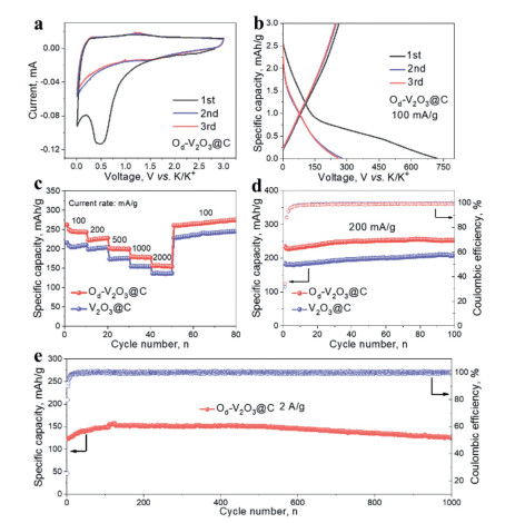
To investigate the benefits of nanostructure and oxygen vacancies, the half-cells performance of as-prepared materials were evaluated at room temperature by the techniques of cyclic voltammetry (CV), galvanostatic charge-discharge (GCD), etc. As depicted in Fig. 3a, CV curves of Od-V2O3@C electrode at 0.1 mV/s exhibit a broad reduction peak at ~0.5 V in the first cycle and then vanish in the subsequent cycles, which results from the formation of solid electrolyte interface (SEI). During the deintercalation process of K+, there is an oxidation peak at ~1.2 V. In the subsequent cycles, the nearly overlapped CV curves suggest the highly reversibility of Od-V2O3@C electrode. At the same time, the CV curves of V2O3@C electrode exhibits the similar trend to the former (Fig. S7 in Supporting information). Fig. 3b displays the typical GCD profiles for the first three cycles of Od-V2O3@C electrode. It delivers an initial discharge/charge capacities of 721.4/262.8 mAh/g, corresponding to a coulombic efficiency (CE) of 36.4%. However, the specific discharge and charge capacities of V2O3@C electrode are only 664.5 and 216.2 mAh/g, respectively, showing a lower CE (32.5%) (Fig. S8 in Supporting information). More importantly, Od-V2O3@C electrode is capable of exhibiting better rate performance than V2O3@C. As illustrated in Figs. 3c and d, the reversible capacities of 262.8, 227.8, 201.5, 179.8, 156.9 mAh/g are achieved at 100, 200, 500, 1000 and 2000 mA/g, respectively. When the current density is switched back to 100 mA/g, a reversible capacity of 261.1 mAh/g is recovered and remains stable in following cycles. In contrast, V2O3@C electrode exhibits inferior specific capacities at corresponding current densities. Such superior rate capability of Od-V2O3@C electrode is further evidenced by the charge/discharge voltage profiles (Fig. S9 in Supporting information). In addition to better rate performance, Od-V2O3@C electrode also exhibits excellent cycling stability. Specifically, Od-V2O3@C electrode maintains a specific capacity of 253 mAh/g after GCD at 200 mA/g for 100 cycles, which is superior to that of V2O3@C (208 mAh/g) (Fig. 3d). Even cycled at 2 A/g, a reversible capacity of 127.4 mAh/g is still retained after 1000 cycles without obvious capacity decay (Fig. 3e). Moreover, the SEM images of Od-V2O3@C electrode after intensely cycling are depicted in Fig. S10 (Supporting information). Impressively, Od-V2O3@C electrode could maintain structural integrity during cycling. This can be ascribed to uniform amorphous carbon shell can protect V2O3 nanoparticles from corrosion of the electrolyte, which guarantees the satisfactory cycling stability. Carbon matrix is essential to achieve high electronic conductivity and mitigate volume change during cycling, and ultimately to achieve higher capacity and better durability. With low carbon content, the beneficial spherical carbon matrix cannot be formed. In order to study the effects of carbon matrix on K-storage performance, a carbon matrix was prepared by dissolving Od-V2O3@C powder in 1 mol/L HNO3 solution and stirring for 24 h, washing with distilled water for several times and drying overnight in a vacuum oven at 80 ℃. The SEM images are shown in Figs. S11a and b (Supporting information), where it is evident that after removal of V2O3, the spherical morphology is still maintained. Besides, the XRD pattern confirms the (002) peak of pure carbon without any peak referred to V2O3 (Fig. S11c in Supporting information). According to the carbon loading (37.7%) in the composite and the stable specific capacity (185 mAh/g at 200 mA/g) of bare carbon, the capacity contribution from carbon in Od-V2O3@C composite is estimated to be 69.7 mAh/g (Fig. S11d in Supporting information).
To further interpret the better rate capability of Od-V2O3@C electrode, the electrochemical kinetics were studied through CV, GITT and EIS measurements. As shown in Fig. 4a, the CV curves of Od-V2O3@C electrode show distinct redox peaks at different scan rates with increasing peak intensity from 0.1 mV/s to 1.0 mV/s. Generally, the peak current (i) vs. scan rate (v) comply with the following equation (Eq. 1) [39]:
|
|
(1) |

where the value of b can evaluate the charge storage behavior of the electrode. As depicted in Fig. 4b, the b values of Od-V2O3@C electrode are close to 1, indicating the capacity is dominated by pseudocapacitance. Besides, the percentages of capacitance and diffusion contributions can be quantitatively calculated according to Eq. 2 [39]:
|
|
(2) |
where k1v and k2v1/2 represent the capacitive contribution fraction and the diffusion one, respectively. As a result, the capacitive contributions occupied ~86.8% of the total capacity at the scan rate of 1.0 mV/s (Fig. S12 in Supporting information). Besides, the ratio of capacitive contribution has a gradual upward tendency with the increase of scan rates, which benefits the high rate performance (Fig. 4c). Although V2O3@C electrode also exhibits dominant surface-controlled capacitive behavior (Fig. S13 in Supporting information), the proportion of capacitive contribution is lower than that of Od-V2O3@C electrode. Therefore, the introduction of oxygen vacancies promotes the capacitance-type charge storage, which accounts for the superior rate capability of Od-V2O3@C electrode. Fig. 4d presents the voltage response of the electrodes under a pulse current density of 50 mA/g. Since the voltage is linearly proportional to τ (Fig. S14b in Supporting information), the K+ diffusion coefficient (DK+) can be obtained by Eq. 3 [40]:
|
|
(3) |
where τ is duration of pulse current, nm is the number of moles, ΔES and ΔEτ are the voltage variation shown in Fig. S14a (Supporting information). The calculated DK+ for Od-V2O3@C and V2O3@C electrodes upon discharge/charge process are shown in Fig. 4e. Apparently, Od-V2O3@C electrode exhibits a much higher diffusion coefficient during the whole process, demonstrating the fast electrochemical kinetics. According to the equivalent circuit model (Fig. S15b in Supporting information), impedance spectra of V2O3@C and Od-V2O3@C electrodes before cycling can be reasonably fitted and depicted in Fig. S15a (Supporting information). As summarized in Table S1 (Supporting information), the values of Ohm impedance (Rs) and charge transfer resistance (Rct) of Od-V2O3@C electrode are 3.2 and 1501 Ω, respectively, which are apparently lower than that of V2O3@C electrode (6.5 and 2361 Ω). These results suggest the fast reaction kinetics of Od-V2O3@C electrode, leading to the better rate capability.
Moreover, four probe method and density functional theory (DFT) calculation is conducted to further understand the impacts on the electronic property of V2O3 after introducing oxygen defects. In order to explore the effects of various oxygen vacancy concentrations on electrical conductivity, Od-V2O3@C materials with different H2 treatment times have been synthesized, and their electrical conductivity were measured by four probe method. As shown in Fig. S16 (Supporting information), the electrical conductivity gradually increases with the extension of treatment times, but then decreases when treatment time is too long. It can conclude that appropriate amount of oxygen vacancy has great influence on the electronic structure of V2O3@C. The open tunnel structure of Od-V2O3@C materials is illustrated in Fig. 5a. As shown in Fig. 5b, the density of states (DOS) of both samples clearly illustrate that the conduction band come across the Fermi levels (0 eV), unveiling the metallic properties of them. Interestingly, the intensity of DOS for Od-V2O3 is substantially higher than that of V2O3, which proves the enhanced electronic conductivity of Od-V2O3. In addition, the band structure also reveals the same conclusion. As shown in Figs. 5c and d, Od-V2O3 possesses a narrower band gap (2.35 eV) than that of V2O3 (2.59 eV), thereby promoting the charge transfer [41, 42].

In conclusion, a rational and feasible approach has been proposed to synthesize Od-V2O3@C anode materials with high performance. The MOF derived carbon coating uniformly wrapping V2O3 nanoparticles can shorten the diffusion distances to enhance the electronic conductivity of materials, as well as alleviate the large volume variation and ensure structural integrity. Moreover, the as-prepared Od-V2O3@C materials with rich oxygen defects is capable of tuning the electronic structure of V2O3 and greatly boosting K+ storage capability. When applied as anode for KIBs, Od-V2O3@C electrode delivers a high capacity of 127.4 mAh/g after cycling for 1000 cycles at high current density of 2 A/g, exhibiting outstanding electrochemical performance. This study provides an effective way for developing advanced anode materials for KIBs.
There are no conflicts to declare.
We gratefully acknowledge the financial support from the National Natural Science Foundation of China (Nos. 51922042 and 51872098) and Fundamental Research Funds for Central Universities, China (No. 2020ZYGXZR074) and the Scientific and Technological Plan of Qingyuan City, China (2019DZX008).
Supplementary material associated with this article can be found, in the online version, at doi:
S.M. Mousavi, M. Zarei, S.A. Hashemi, et al., Potassium Ion Batter. Mater. Appl. (2020) 43–98.
Y. Li, Y. Lu, C. Zhao, et al., Energy Storage Mater. 7 (2017) 130–151. doi: 10.1016/j.ensm.2017.01.002
B. Scrosati, J. Hassoun, Y. -. K. Sun, Energy Environ. Sci. 4 (2011) 3287–3295. doi: 10.1039/c1ee01388b
S.W. Kim, D.H. Seo, X. Ma, et al., Adv. Energy Mater. 2 (2012) 710–721. doi: 10.1002/aenm.201200026
Q. Zhang, Z. Wang, X. Li, et al., Chem. Eng. J. 431 (2021) 133456.
X. Wu, D.P. Leonard, X. Ji, Chem. Mater. 29 (2017) 5031–5042. doi: 10.1021/acs.chemmater.7b01764
Q. Deng, F.H. Zheng, W.T. Zhong, et al., Chem. Eng. J. 392 (2020) 12375.
Y. Liu, Q. Deng, Y. Li, et al., ACS Nano 15 (2021) 1121–1132. doi: 10.1021/acsnano.0c08094
Y. Xia, W. Jin, Y. Qi, et al., Chin. Chem. Lett. 32 (2021) 2433–2437. doi: 10.1016/j.cclet.2021.01.025
K. Lei, F. Li, C. Mu, et al., Energy Environ. Sci. 10 (2017) 552–557. doi: 10.1039/C6EE03185D
S. Komaba, T. Hasegawa, M. Dahbi, et al., Electrochem. Commun. 60 (2015) 172–175. doi: 10.1016/j.elecom.2015.09.002
W. Zhang, Y. Liu, Z. Guo, Sci. Adv. 5 (2019) eaav7412. doi: 10.1126/sciadv.aav7412
X. Zou, P. Xiong, J. Zhao, et al., Phys. Chem. Chem. Phys. 19 (2017) 26495–26506. doi: 10.1039/C7CP03852F
X. Min, J. Xiao, M. Fang, et al., Energy Environ. Sci. 14 (2021) 2186–2243. doi: 10.1039/D0EE02917C
W. Zhu, A. Li, Z. Wang, et al., Small 17 (2021) 2006424. doi: 10.1002/smll.202006424
Y. Li, W. Zhong, C. Yang, et al., Chem. Eng. J. 358 (2019) 1147–1154. doi: 10.1016/j.cej.2018.10.135
A.P. Cohn, N. Muralidharan, R. Carter, et al., J. Mater. Chem. A 4 (2016) 14954–14959. doi: 10.1039/C6TA06797B
B. Xu, S. Qi, F. Li, et al., Chin. Chem. Lett. 31 (2020) 217–222. doi: 10.1016/j.cclet.2019.10.009
V. Gabaudan, R. Berthelot, L. Stievano, et al., J. Phys. Chem. C 122 (2018) 18266–18273. doi: 10.1021/acs.jpcc.8b04575
J. Huang, X. Lin, H. Tan, et al., Adv. Energy Mater. 8 (2018) 1703496. doi: 10.1002/aenm.201703496
W. Zhang, W. Huang, Q. Zhang, Chem. Eur. J. 27 (2021) 6131–6144. doi: 10.1002/chem.202005259
Y. Liang, C. Luo, F. Wang, et al., Adv. Energy Mater. 9 (2019) 1802986. doi: 10.1002/aenm.201802986
J. Zhou, H. Zhao, Q. Zhang, et al., Chem. Commun. 55 (2019) 1406–1409. doi: 10.1039/C8CC09205B
Y. Li, Q. Zhang, Y. Yuan, et al., Adv. Energy Mater. 10 (2020) 2000717. doi: 10.1002/aenm.202000717
D. Xu, L. Chen, X. Su, et al., Adv. Funct. Mater. 32 (2022) 2110223. doi: 10.1002/adfm.202110223
C. Hu, K. Ma, Y. Hu, et al., Green Energy Environ. 6 (2021) 75–82. doi: 10.1016/j.gee.2020.02.001
Y. Li, C. Yang, F. Zheng, et al., Nano Energy 59 (2019) 582–590. doi: 10.1016/j.nanoen.2019.03.002
T. Jin, H. Li, Y. Li, et al., Nano Energy 50 (2018) 462–467. doi: 10.1016/j.nanoen.2018.05.056
F. Chen, S. Wang, X.D. He, et al., J. Mater. Chem. A 8 (2020) 13261–13266. doi: 10.1039/D0TA01057J
J. Hu, Y. Xie, J. Zheng, et al., ACS Appl. Mater. Interfaces 13 (2021) 12149–12158. doi: 10.1021/acsami.1c01303
J. Lu, C. Wang, G. Xia, et al., J. Mater. Chem. A 8 (2020) 23939–23946. doi: 10.1039/D0TA08845E
J. Cao, D. Zhang, Y. Yue, et al., Nano Energy 84 (2021) 105876. doi: 10.1016/j.nanoen.2021.105876
X. Deng, K. Zou, R. Momen, et al., Sci. Bull. 66 (2021) 1858–1868. doi: 10.1016/j.scib.2021.04.042
Q. Gan, H. He, Y. Zhu, et al., ACS Nano 13 (2019) 9247–9258. doi: 10.1021/acsnano.9b03766
Y. Ding, Y. Peng, S. Chen, et al., ACS Appl. Mater. Interfaces 11 (2019) 44109–44117. doi: 10.1021/acsami.9b13729
Y. Li, K. Xiao, C. Huang, et al., Nano Micro Lett. 13 (2021) 1. doi: 10.1007/s40820-020-00525-y
S. Petnikota, J.J. Toh, J.Y. Li, et al., ChemElectroChem 6 (2019) 493–503. doi: 10.1002/celc.201801244
H. Luo, B. Wang, C. Wang, et al., Energy Storage Mater. 33 (2020) 390–398. doi: 10.1016/j.ensm.2020.08.011
N. Liu, X. Wu, L. Fan, et al., Adv. Mater. 32 (2020) 1908420. doi: 10.1002/adma.201908420
S. Zhao, K. Yan, P. Munroe, et al., Adv. Energy Mater. 9 (2019) 1803757. doi: 10.1002/aenm.201803757
Q. Deng, Q. Cheng, X. Liu, et al., Chem. Eng. J. 430 (2022) 132710. doi: 10.1016/j.cej.2021.132710
H. Geng, M. Cheng, B. Wang, et al., Adv. Funct. Mater. 30 (2020) 1907684. doi: 10.1002/adfm.201907684

Figure 1 (a, b) SEM images, (c) TEM image, (d) HRTEM image, (e) SAED pattern, (f) EDX elemental mapping of Od-V2O3@C materials.

Figure 2 (a) XRD patterns, (b) Raman spectra, (c) TGA curves, (d, e) high resolution XPS spectra of (d) V 2p, (e) O 1s, and (f) EPR spectra of Od-V2O3@C and V2O3@C materials.

Figure 3 (a) CV curves of Od-V2O3@C electrode at 0.1 mV/s. (b) GCD curves of Od-V2O3@C electrode at 100 mA/g for first three cycles. (c) Rate capability of Od-V2O3@C and V2O3@C electrodes at various current density. (d) Cycling stability of Od-V2O3@C and V2O3@C electrodes at 200 mA/g. (e) Long-term cycling life of Od-V2O3@C electrode at 2 A/g.

Figure 4 (a) CV curves at various scan rates of Od-V2O3@C electrode. (b) log(i) vs. log(v) plots and corresponding linear relationship of Od-V2O3@C electrode. (c) Normalized contribution ratios of capacitive contribution at various scan rates of Od-V2O3@C electrode. (d) GITT curves at a pulse current density of 50 mA/g of Od-V2O3@C and V2O3@C electrodes. (e) The calculated K+ diffusion coefficients upon discharge and charge process of Od-V2O3@C and V2O3@C electrodes.

 扫一扫看文章

扫一扫关注我们
 DownLoad:
 下载:
下载:

 下载:
下载: