Key Laboratory of Nanosystem and Hierarchical Fabrication, CAS Center for Excellence in Nanoscience, National Center for Nanoscience and Technology, Beijing 100190, China
b.
Center of Materials Science and Optoelectronics Engineering, University of Chinese Academy of Sciences, Beijing 100049, China
c.
School of Material Science and Engineering, Zhengzhou University, Zhengzhou 450001, China
sunxn@nanoctr.cn (X. Sun). 1 These authors contributed equally to this work.
Received Date:
26 January 2022 Accepted Date:
07 March 2022 Revised Date:
15 February 2022 Available Online:
15 March 2023
Abstract:
In the field of organic phototransistor, achieving both broad-spectral and high photosensitivity has always been a big challenge. The innovation of device structure has previously proven to be a possible solution to this problem. Here in this study, a novel organic phototransistor based on a high mobility n-type small molecule as the conducting layer and an isolated bulk heterojunction light-absorbing layer as the floating gate has been demonstrated in this study. With the special designed device structure, the phototransistor shows extremely high sensitivity to broad spectral and weak light irradiation, and the photoresponsivity and photocurrent/dark-current ratio of the device can reach up to 4840 mA/W and 1.8 × 10⁵ respectively. For conclusion, this study suggests a potential way to obtain high-performance phototransistors at room temperature, which will further promote the commercial application of organic phototransistors.
Thanks to the flourishing development of organic semiconductors with excellent photoelectric properties [1-3], organic electronic devices have shown potential applications in the field of photoelectric detection [4-7]. In particular, organic phototransistors (OPTs) based on field-effect transistors structure, are endowed with the functionality of converting optical signal into electrical signal for detection [8-10], which have exhibited wide application prospects in medical imaging, optical remote sensing, image sensors, and environmental monitoring [11-14]. In OPTs, the incident light signal is capable of controlling the electrical properties of the devices by amplifying the source-drain current (IDS). Furthermore, the photogeneration and the dissociation of the excitons, the utmost important preconditions for the photoresponse property, can be promoted by the electric field induced by gate voltage (VGS) [15, 16]. An OPT, integrating photoelectric conversion capacity of organic solar cells and signal amplification function of field-effect transistor into a single device [17], has higher photoresponse sensitivity and lower noise current compared to photodiodes and photoconductors [18]. Great progresses have been made to realize the effective photocontrol of device electric properties through incorporating photosensitive organic semiconductors as conducting layers in OPTs [10, 15, 19-21]. However, to achieve high photosensitivity and broad spectral response is still a big challenge because of the difficulty that reaching a balance between charge transport and light absorption [22, 23].
Considerable research efforts on organic phototransistors have been devoted to tackle this challenge. For example, interfacial modification engineering [24] and active materials doping [25] are able to improve the carrier mobility and enhance the photosensitivity by charge trap effect [26]. But these strategies are hardly to broaden the detectable spectrum range because adjusting the spectral absorption properties in these material systems is unavailable. Designing ideal photoactive materials with excellent charge transport properties and strong spectral response at wide wavelength ranges is an optimal solution in the research of OPTs [22, 27]. Nevertheless, it is difficult to design and synthesize suitable semiconducting materials by controlling molecular structure [28]. In this regard, more attention has been paid to finding new solutions from the device architecture [29-31]. Huang et al. reported a high-performance floating-gate organic phototransistor (FGOPT) with the bulk heterojunction (BHJ) and a high mobility p-type organic semiconductor 2,7-dioctyl[1]-benzothieno[3,2-b][1]benzothiophene (C8-BTBT) as the light-absorbing layer and the hole transport layer respectively [32]. Yang et al. realized ultrahigh photosensitivity and broad spectral response phototransistors based on the structure of BHJ and an ultrathin oxide semiconductor [33]. These studies have provided a promising research direction in fabricating high-performance OPTs, that is the combination of BHJ light-absorbing layer and high-mobility conducting layer to realize sensitive and broad spectral photodetectivity [13, 34]. To date, there are very few researches focusing on the electron transport in the channel of OPTs because high-performance FGOPT that incorporates BHJ structure and n-type organic small molecule has not been reported yet.
In this paper, we choose the n-type organic semiconductor core-expanded naphthalene diimides (NDI3HU-DTYM2) with large charge mobility and ambient stability as conducting layer, and firstly combine it with the BHJ photoactive layer to fabricate FGOPT. This special floating-gate structure [32] fully exhibits both advantages of broad spectral absorption of BHJ and excellent charge transport of NDI3HU-DTYM2. As expected, the fabricated phototransistors exhibit high photoresponsivity 4840 mA/W under weak light and maximum photocurrent/dark-current ratio as high as 1.8 × 10⁵. In addition, the device exhibits remarkable operation stability and reliable accuracy in the photoelectric detection under different light intensities. This FGOPT with the combination of BHJ and n-type small molecule has a significant impetus for the future development of flexible photo-sensing devices.
The schematic structure of the proposed FGOPT in this article is shown in Fig. 1a. It is based on the bottom-gate-top-contact organic filed-effect transistor structure. The overall FGOPT is composed of gate electrode, bottom dielectric layer, light-absorbing layer, top insulating layer, conducting layer and source-drain electrodes, which are sequentially deposited from bottom to top (more details are seen in Supporting information). The P3HT: PC61BM layer, the most-studied photoactive materials for the BHJ-structured organic solar cell [35], acts as a light-absorbing layer of FGOPT. The role of light-absorbing layer is to broaden the absorption spectrum range and improve photoelectric conversion efficiency. The Parylene C film possesses excellent insulating property and robust chemical resistance [36], and thus can protect the light-absorbing layer from solvent destruction during spin-coating the conducting layer. The n-type small-molecule semiconductor NDI3HU-DTYM2, due to high mobility of up to 1.2 cm2 V−1 s−1 and stable electrical properties [37], is selected as conducting layer material, which provides an excellent electron transport guarantee for the FGOPT. The chemical structures of molecular materials used in this work are shown in Fig. 1b.
Figure 1
Figure 1.
(a) Schematic diagram of fabricated floating-gate organic phototransistors (FGOPT). (b) Chemical structures of the molecular materials used in the work. (c) Energy level diagram for the P3HT: PC61BM heterostructure junction (BHJ), and illustration for the processes of excitons generation, charge separation and transfer in the light-absorbing layer under light irradiation. (d) Ultraviolet and visible (UV–vis) absorption spectra of Parylene C (green), NDI3HU-DTYM2 (purple), P3HT: PC61BM (red), P3HT: PC61BM/Parylene C/NDI3HU-DTYM2 (blue) films.
The energy level diagram for the P3HT: PC61BM BHJ system in our FGOPT is shown in Fig. 1c. The lowest unoccupied molecular orbital (LUMO) energy levels are −3.0 and −4.3 eV for P3HT and PC61BM, respectively. The LUMO-LUMO deviation is larger than 0.3~0.5 eV (the energy that needs for the electron transfer) [38]. And the processes of excitons generation and spatial dissociation in the P3HT: PC61BM BHJ films under light irradiation are shown in Fig. 1c [39]. The excitons are generated in the light-absorbing layer and dissociated into free electrons and holes at donor/accepter interfaces, and then these electrons and holes drift towards the opposite sides under the electric field induced by VGS. The holes separated from excitons accumulate on the interface between top dielectric and conducting layer, while the electrons heap at the bottom dielectric and light-absorbing layer interface. Electrons in the n-type conducting channel are constrained by photogenerated holes, and thus gives rise to the increase of IDS and shift of threshold voltage (Vth). The ultraviolet and visible (UV–vis) absorption spectra of the Parylene C, the NDI3HU-DTYM2, the P3HT: PC61BM and the P3HT: PC61BM/Parylene C/NDI3HU-DTYM2 films deposited on quartz substrates are shown in Fig. 1d. There is no obvious characteristic peak in the range of 300–800 nm for Parylene C film, reflecting the excellent optical transparency. The obvious and sharp absorption peak of NDI3HU-DTYM2 film is observed at around 600 nm and very weak intensity peaks discretely appear at 300~380 and 530 nm, while that of P3HT: PC61BM film covers a wide wavelength at 300~600 nm. Due to presence of light-absorbing layer, the P3HT: PC61BM/Parylene C/NDI3HU-DTYM2 film exhibits a wider and stronger intensity absorption spectrum than NDI3HU-DTYM2 film. This indicates that the light-absorbing layer is significant for expanding the spectral range of photoresponse.
The photoresponse properties of FGOPT with 58 nm light-absorbing layer is reflected by the representative transfer characteristics measured under dark and different light intensities (32.4, 244, 551, 984 and 2065 µW/cm2) at drain-source bias VDS = 5 V as shown in Fig. 2a. IDS of FGOPT increases with increasing positive VGS under positive VDS, indicating a typical n-channel transport mode. Compared with the transfer characteristic of FGOPT measured in the dark, we find that transfer characteristics under various light intensities present substantial IDS change and obvious Vth shifts, which are typical photoresponse behaviors of the FGOPT. The amplification of IDS and shifts of Vth are attributed to the photoelectric conversion process in light-absorbing layer under light illumination [10]. Moreover, FGOPT exhibits different degrees of photoresponse behavior under different light intensities since the density of photogenerated charge carrier is proportional to incident light intensities [40]. Notably, IDS of FGOPT exhibits maximum increasement of ~300 nA under weak light illumination (32.4 µW/cm2) compared with that measured in dark environment (Fig. 2b). This signifies that our constructed FGOPT is very sensitive to weak light illumination.
Figure 2
Figure 2.
Photoresponse performances of FGOPT. (a) Typical transfer characteristics of the FGOPT with 58 nm light-absorbing layer measured under dark and various light intensities, 32.4, 244, 551, 984 and 2065 µW/cm2 respectively. (b) Change of IDS under weak light intensity (32.4 µW/cm2) compared with that in the dark.
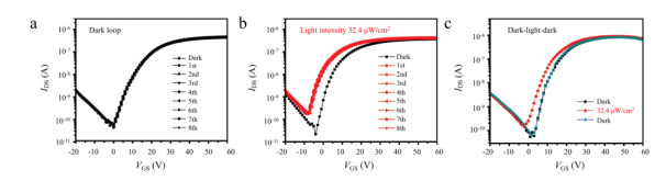
Due to the excellent electrical stability of conducting layer NDI3HU-DTYM2 and light-absorbing layer P3HT: PC61BM [35, 37], the constructed FGOPTs based on above materials should present high stability. To investigate the stability of FGOPTs, firstly, the transfer characteristics are circularly measured in the dark environment. As shown in Fig. 3a, after eight times measurements in the dark, transfer characteristics completely coincide with initial curve. This excellent electrical stability of FGOPT under dark provides a significant precondition of accurate photoresponse measurement of FGOPTs because the measurement errors caused by the device instability is effectively eliminated.
Figure 3
Figure 3.
Stability and accuracy measurements of FGOPT devices. (a) Cyclic measurements of transfer characteristics in the dark environment. (b) Cyclic measurements of transfer characteristics under weak light intensity of 32.4 µW/cm2. (c) Dark-light-dark transfer characteristic measurements under weak light intensity of 32.4 µW/cm2.
To examine the stability and accuracy of the FGOPT under light irradiation, we circularly measure the transfer characteristics under weak light intensity of 32.4 µW/cm2 (Fig. 3b) and stronger light intensity of 244 µW/cm2 (Fig. S1a in Supporting information). The transfer characteristics of FGOPT under the weak light intensity (32.4 µW/cm2) and 244 µW/cm2 both show equivalent variation of current and Vth shift comparing with that in dark. This indicates excellent stability and accuracy of FGOPT in the photoelectric conversion process and photocurrent detection. In addition, we study the reversibility of photoresponse behavior by dark-light-dark measurements under light intensity of 32.4 and 244 µW/cm2 (Fig. 3c and Fig. S1b in Supporting information). We find that the transfer characteristics of FGOPT can restore to its original dark state after that measured under light illumination. This is because that generated photocurrent in the light-absorbing layer immediately disappears once removed the illumination.
In addition, the thickness of the light-absorbing layer has a significant impact on photoelectric conversion efficiency in solar cells [41], therefore, we fabricate FGOPTs with different-thickness (90 nm, 36 nm) light-absorbing layer to compare the photoresponse performances. As shown in Fig. S2 (Supporting information), we observe that the transfer characteristics with various light intensities of all FGOPTs gradually overlap when applying higher gate voltage. It can be explained that in this condition, the higher VGS makes the FGOPTs at on-state, and thus the most charge carriers in conducting layer induced by VGS will dominate the IDS of FGOPTs, while charge carriers generated in light-absorbing layer have a very limited influence on IDS.
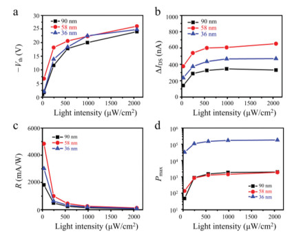
The photoresponse sensitivity of FGOPTs can be characterized by parameters: the shift of Vth, photocurrent (∆IDS), photoresponsivity (R) and photocurrent/dark-current ratio (P). The photoresponse sensitivity of FGOPTs with different light-absorbing layer thickness is summarized in Fig. 4. As seen in Fig. 4a, Vth of FGOPTs with different-thickness light-absorbing layers shows conformably shift towards negative value with increasing light intensities. We infer that the accumulated holes serve as pitfalls to trap electrons due to the coulomb interaction on the interface between the top dielectric layer and the light-absorbing layer, leading to the pronounced shift of Vth [32]. ∆IDS is defined as the IDS discrepancy under illumination and dark. The extracted ∆IDS of FGOPTs with different-thickness light-absorbing layers as a function of light intensities is shown in Fig. 4b. It can be seen that ∆IDS of FGOPTs significantly enhances with increasing light intensity below 551 µW/cm2, and then reaches a plateau as the light intensity is above 551 µW/cm2. This indicates that the ∆IDS is saturated in this condition. Furthermore, we note that ∆IDS of FGOPTs with 58 nm-thickness light-absorbing layer is up to 600 nA under the light intensity above 551 µW/cm2, which is larger than that of FGOPTs with 36 nm and 90 nm light-absorbing layers.
Figure 4
Figure 4.
The photoresponse sensitivity of FGOPTs with different-thickness light-absorbing layers at VDS = 5 V. (a) Threshold voltage (Vth), (b) photocurrent (∆IDS) and (c) photoresponsivity (R) as a function of light intensity at VGS = 21 V. (d) The maximum photocurrent/dark-current ratio (P) of FGOPTs with 90 nm-thickness light-absorbing layer (at VGS = −2 V), 58 nm-thickness light-absorbing layer (at VGS = 0 V) and 36 nm-thickness light-absorbing layer (at VGS = 10 V) as a function of light intensity.
R and P are another two important parameters to evaluate the photoresponse sensitivity of phototransistors, which represent the capability of photoelectric conversion. R and P can be calculated by the following equations:
(1)
(2)
where Iph is ∆IDS of FGOPT, Ilight and Idark are the IDS under illumination and in the dark respectively, Popt is the irradiation intensity on the channel of FGOPTs, Pinc is the illumination intensity density, and A is the effective irradiated area on the devices. R of FGOPTs with varied-thicknesses light-absorbing layer is summarized in Fig. 4c. The maximum R reaching up to 4840 mA/W appears at devices with 58 nm light-absorbing layer under weak light intensity of 32.4 µW/cm2, indicating excellent capability of photoelectric conversion under weak light. To reveal the best photoelectric performance of devices, the maximum P of FGOPTs with different-thicknesses light-absorbing layers at their corresponding VGS is summarized in Fig. 4d. It shows that Pmax of all devices can reach higher than 103 at light illumination exceeding 244 µW/cm2. In addition, Pmax displays insignificant changes with the light intensity above 551 µW/cm2. This variation tendency of Pmax is consistent with the variation of ∆IDS in Fig. 4b. The maximum P is 1.8 × 10⁵, which can be obtained in FGOPTs with 36 nm-thickness light-absorbing layer. This is attributed to its very low off-state current below 2 pA, because the smaller off-state current and the larger ∆IDS are preconditions for a high photosensitive phototransistor in weak light [42].
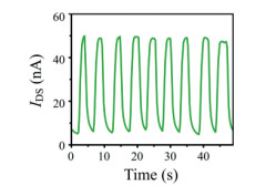
To further corroborate the potential of this FGOPT in the field of optoelectronic applications, the switching behavior of FGOPT is investigated. The influence of light illumination on FGOPT as time-dependent at VGS = 10 V and VDS = 10 V is shown in Fig. 5. We find that IDS increases by 40 nA with a light intensity of 2.06 mW/cm2 at a low operation voltage. The devices exhibit a highly reproducible and sensitive photoresponse to the light on-off switching. Furthermore, the ∆IDS has no obvious attenuation under the same illumination during the measurement of switching behavior, indicating the excellent stability of our device.
Figure 5
Figure 5.
The on-off switching behavior of FGOPTs under illumination of 2.06 mW/cm2. The IDS is measured at VGS = 10 V and VDS = 10 V.
In summary, we have successfully constructed the FGOPTs based on the combination of n-type small molecule semiconductor NDI3HU-DTYM2 and P3HT: PC61BM BHJ. We attempted to optimize the devices from the perspective of adjusting the thickness of the light-absorbing layers. The devices with 58 nm light-absorbing layer exhibited larger ∆IDS under the same light intensity due to the better photoelectric conversion efficiency, obtaining maximum R of 4840 mA/W. While the phototransistors with 36 nm light-absorbing layer exhibited the higher Pmax owing to the lower off-state current, obtaining maximum P of 1.8 × 10⁵. Moreover, FGOPTs were demonstrated to show excellent stability and accuracy under dark and light illumination. All in all, these results have provided a feasible method for fabricating high-sensitivity photoresponse OPTs.
Declaration of competing interest
The authors report no declarations of interest.
Acknowledgments
This work is supported financially by the Ministry of Science and Technology of the People's Republic of China (No. 2017YFA0206600), the National Natural Science Foundation of China (Nos. 52050171, 51822301, 22175047, 52103203, and 91963126), the CAS Instrument Development Project (No. YJKYYQ20170037), the Strategic Priority Research Program of the Chinese Academy of Sciences (No. XDB36020000), the CAS Pioneer Hundred Talents Program, the Natural Science Foundation of Shandong Province (No. ZR2020ME070), and China Postdoctoral Science Foundation (No. 2021M690802).
Supplementary materials
Supplementary material associated with this article can be found, in the online version, at doi:10.1016/j.cclet.2022.03.029.
[1]
S. Fratini, M. Nikolka, A. Salleo, G. Schweicher, H. Sirringhaus, Nat. Mater. 19 (2020) 491–502. doi: 10.1038/s41563-020-0647-2
Figure 1
(a) Schematic diagram of fabricated floating-gate organic phototransistors (FGOPT). (b) Chemical structures of the molecular materials used in the work. (c) Energy level diagram for the P3HT: PC61BM heterostructure junction (BHJ), and illustration for the processes of excitons generation, charge separation and transfer in the light-absorbing layer under light irradiation. (d) Ultraviolet and visible (UV–vis) absorption spectra of Parylene C (green), NDI3HU-DTYM2 (purple), P3HT: PC61BM (red), P3HT: PC61BM/Parylene C/NDI3HU-DTYM2 (blue) films.
Figure 2
Photoresponse performances of FGOPT. (a) Typical transfer characteristics of the FGOPT with 58 nm light-absorbing layer measured under dark and various light intensities, 32.4, 244, 551, 984 and 2065 µW/cm2 respectively. (b) Change of IDS under weak light intensity (32.4 µW/cm2) compared with that in the dark.
Figure 3
Stability and accuracy measurements of FGOPT devices. (a) Cyclic measurements of transfer characteristics in the dark environment. (b) Cyclic measurements of transfer characteristics under weak light intensity of 32.4 µW/cm2. (c) Dark-light-dark transfer characteristic measurements under weak light intensity of 32.4 µW/cm2.
Figure 4
The photoresponse sensitivity of FGOPTs with different-thickness light-absorbing layers at VDS = 5 V. (a) Threshold voltage (Vth), (b) photocurrent (∆IDS) and (c) photoresponsivity (R) as a function of light intensity at VGS = 21 V. (d) The maximum photocurrent/dark-current ratio (P) of FGOPTs with 90 nm-thickness light-absorbing layer (at VGS = −2 V), 58 nm-thickness light-absorbing layer (at VGS = 0 V) and 36 nm-thickness light-absorbing layer (at VGS = 10 V) as a function of light intensity.


 DownLoad:


 下载:
下载:


 下载:
下载:
