Citation:
Huimin Yue, Wenxiang Wang, Kun Wang, Yongqi Liu, Yang Liu, Junan Pan, Xia Liu, Longlu Wang. Epitaxial growth along with atomic substitution for efficient solar hydrogen production[J]. Chinese Chemical Letters,
2026, 37(11): 111726.
doi:
10.1016/j.cclet.2025.111726
Epitaxial growth along with atomic substitution for efficient solar hydrogen production
English
Epitaxial growth along with atomic substitution for efficient solar hydrogen production
College of Chemistry and Chemical Engineering, Qingdao University, Qingdao 266071, China
b.
College of Electronic and Optical Engineering & College of Flexible Electronics (Future Technology), Nanjing University of Posts & Telecommunications (NJUPT), Nanjing 210023, China
Received Date:
24 June 2025 Accepted Date:
14 August 2025 Revised Date:
08 August 2025 Available Online:
15 November 2026
Abstract:
Strong interfacial coupling between a semiconductor photocatalyst and a cocatalyst is crucial for enhancing photocatalytic hydrogen production. This study employs an anion exchange strategy to construct atomically thin two-dimensional MoSe2 nanosheets on one-dimensional CdS nanorods, achieving strong interfacial coupling for effective hydrogen production. Consequently, the CdS@MoSe2 heterojunctions exhibits a high H2 evolution rate of 15 mmol h−1 g−1 and an apparent quantum yield of 65% at 420 nm. This remarkable performance is attributed to the well-defined interface structure, in which chemical bonds are formed via strain-driven atomic substitution. The detailed interface structure between CdS and MoSe2 is clearly revealed through experimental characterizations, while the substitution process is thoroughly explained using theoretical methods. This work introduces a novel approach for optimizing the structure and quality of nanohybrid interfaces via strain-driven atomic substitution.
In addition to the electrochemical hydrogen evolution reaction (HER), solar-driven hydrogen production stands out as a highly promising method for efficiently converting solar energy into chemical fuel. The performance of photocatalysts relies not only on their intrinsic properties, such as atomic structure, electronic structure, and electron affinity, but also on the interfacial coupling between the photocatalyst and cocatalyst [1-5]. Engineering advanced photocatalysts through the hybridization of two or more materials is an effective strategy to overcome the limitations of individual components, boost performance, and potentially unlock new functionalities for practical applications [6-9]. For efficient hydrogen production, spatial integration of the photocatalyst and cocatalyst to achieve strong interfacial coupling is critical. A well-defined interface enhances light absorption and promotes charge carrier separation in photocatalysts [10-12]. Ideally, such an interface would also provide efficient charge transfer and trapping channels for the separation of photo-generated electron-hole pairs. While considerable effort has been devoted to the development of transition metal dichalcogenide (TMD) nanosheet-based hybrid photocatalysts [13-18], most pioneering studies have focused on the simple hybridization of TMD nanosheets without sufficient control over interface architectures. Zhang et al. reported a feasible synthetic approach to create edge-epitaxial MoS2/CdS nanorod (NR) hybrids, where CdS NRs served as sacrificial scaffolds to match the lattice constants [19]. This was followed by defect-induced overgrowth of [001]-oriented MoS2 ribbons on [0001]-oriented CdS nanorods, leading to the formation of an epitaxial structure. It is important to note that when CdS is used as a building block, particularly under extreme conditions such as high temperatures or in the presence of strong reducing and oxidizing agents, surface etching can easily occur during the hybrid material preparation process [20-25]. Existing CdS-based photocatalysts for hydrogen evolution suffer from critical limitations in interfacial coupling and charge separation efficiency. Conventional CdS/cocatalyst systems exhibit weak interfacial contacts, causing cocatalyst detachment, lattice mismatch defects, and insufficient chemical bonding. These flaws lead to severe charge recombination and suboptimal performance, typically manifesting as low HER rates, quantum efficiencies, and short-term stability. Such deficiencies arise from unoptimized band alignment and interfacial trap states, highlighting an unmet need for atomic-level interface engineering. Strong interfacial coupling can be established through chemical bonding when CdS is used as a building block to construct heterojunctions.
In this work, a strong interfacial interaction was established through an anion exchange reaction during the overgrowth of MoSe2 nanosheets (NSs) on CdS nanorods (NRs), forming an epitaxial structure. This structure facilitates an anion exchange between MoSe2 and CdS, leading to delocalized interface states at the MoSe2/CdS heterointerface. These states significantly reduce ohmic losses and enhance electron transport efficiency from CdS to MoSe2, thereby greatly improving photocatalytic hydrogen evolution under visible light. The outstanding hydrogen evolution performance and stability of the MoSe2/CdS heterojunctions are attributed to the distinctive structure and properties of CdS@MoSe2, which enhance charge transport and suppress electron-hole recombination, allowing more electrons to participate in hydrogen production. Both experimental data and density functional theory (DFT) calculations confirm that the high efficiency of solar hydrogen production arises from the strong interfacial interaction between CdS and MoSe2. The enhanced catalytic activity is further attributed to the creation of unsaturated hydrogen evolution reaction active sites in MoSe2, facilitated by the anion exchange reaction.
The typical synthesis of the CdS@MoSe2 heterojunction and the mechanism of S substitution by MoSe2 are schematically depicted in Figs. S1 and S2 (Supporting information). As shown in Fig. S2a, the CdS@MoSe2 heterojunction was synthesized using a two-step solvothermal method. First, CdS NRs were synthesized by reacting cadmium acetate with sulfur powder in ethylenediamine. MoSe2 NSs were then grown in situ on the CdS NRs via a simple hydrothermal approach, employing ammonium molybdate as the molybdenum precursor, sulfur powder as the sulfur source, and hydrazine hydrate as a reducing agent in deionized water. During the hydrothermal process, the surface atoms of the CdS NRs become active and migrate into the crystalline lattice of MoSe2 NSs, resulting in sulfur doping of MoSe2 with reduced crystallinity. Detailed information on the preparation process can be found in the Experimental Section (Supporting information). The MoSe2 loading can be easily adjusted by varying the amounts of its precursors. To better understand the Se-S atomic substitution process, the most probable pathway was calculated, including the initial, transition, and final states (IS, TS, FS), as shown in Fig. S2b. The calculation revealed that the S atom initially adsorbs on top of a Se atom and then migrates to a neighboring Se atom. This leads to the displacement of the adjacent S atom, lifting it off the surface of MoSe2. The transition state (TS) of the substitution process occurs when the Se and S atoms are nearly at the same vertical level. Subsequently, the Se atom occupies the neighboring S position, pushing the displaced S atom to an adjacent site. This entire pathway requires an activation energy of 2.6 eV, as shown in Fig. S2c. The substitution barrier is also influenced by the strain field. Fig. S2d illustrates how the substitution barrier evolves as a function of strain, revealing that strain induced by lattice matching significantly lowers the substitution barriers. This strain-driven substitution mechanism helps explain the observed anion exchange phenomenon. The insights gained from this strain-driven atomic substitution mechanism provide valuable understanding into the kinetic processes of atomic diffusion and exchange in well-defined interface structures, which are crucial for the precise preparation of strong interfacial coupling.
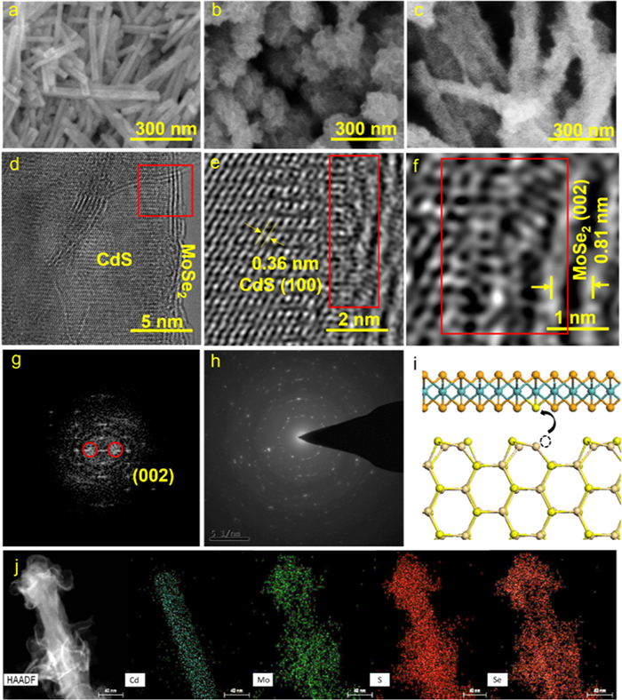
SEM images of the pure CdS NRs are shown in Fig. 1a, where the diameters of the highly uniform 1D CdS NRs range from 30 nm to 50 nm, with smooth surfaces and no visible material adhered to them. As illustrated in Fig. 1b, when CdS NRs are not used as growth templates, MoSe2 nanosheets tend to cluster together, forming micron-sized platelet-like structures. In contrast, Fig. 1c demonstrates that when CdS NRs are introduced, MoSe2 grows uniformly on their surfaces. Fig. 1d further highlights that the high-crystallinity 1D CdS NRs are coated with a thin shell of few-layer MoSe2 nanosheets, with a distinct interface clearly visible between the CdS core and the MoSe2 shell. The extensive interfacial contact between the core and shell in these core-shell structures results in the formation of heterojunctions. The strong interfacial coupling effectively enhances the separation of photogenerated electron-hole pairs and facilitates the transfer of photogenerated carriers, thus significantly improving photocatalytic hydrogen evolution (HER) performance. The atomically thin MoSe2 nanosheets offer several advantages for separating and transferring photogenerated carriers.
Figure 1
Figure 1.
SEM images of (a) pure CdS, (b) MoSe2 and (c) CdS@MoSe2 heterojunctions. (d-f) TEM images of CdS@MoSe2 heterojunctions (g) The FFT pattern taken at the circle in (d). (h) SAED pattern of CdS@MoSe2 heterojunctions. (i) Schematic model of the anion exchange. (j) HAADF-STEM and the corresponding STEM-EDS images of Cd, Mo, S and Se in CdS@MoSe2 heterojunctions with 5 wt% ratios of MoSe2.
According to the diffusion equation t = d2/k2D, where d represents particle size, k is a constant, and D is the diffusion coefficient of electron-hole pairs, the ultrathin nature of MoSe2 reduces the diffusion length of charge carriers, allowing them to migrate more rapidly. This shorter migration distance reduces the recombination probability of electrons and holes, enabling a greater proportion of carriers to reach the catalyst surface. Consequently, atomically thin 2D catalysts have been explored for their ability to enhance the separation efficiency of photogenerated electron-hole pairs, resulting in improved photocatalytic activity. Fig. 1e presents a high-resolution TEM (HRTEM) image of the CdS@MoSe2 heterojunctions, showing two distinct lattice stripes with spacings of 0.34 and 0.81 nm, corresponding to the (100) facet of hexagonal CdS NRs and the (002) facet of MoSe2, respectively. As shown in Fig. S3 (Supporting information), X-ray diffraction (XRD) of CdS@MoSe2 further confirms that CdS has a high degree of crystallinity. Compared to the well-crystallized CdS NRs, the lattice spacing associated with the MoSe2 layer is less distinct, indicating lower crystallinity of MoSe2 in the composite. The highly disordered surface atoms in MoSe2 are likely to serve as catalytically active sites. Fig. 1f shows a heterojunction analysis of the CdS@MoSe2 nanosheets-on-nanorods structure, where a visible transition region between the hexagonal CdS phase and the MoSe2 phase is clearly observed at the interface. The atomic-level chemical bonding at this interface minimizes traps and non-productive recombination, ensuring efficient separation and transfer of photoexcited carriers, thereby enhancing photocatalytic performance. TEM analysis confirms the successful synthesis of well-defined 1D CdS NRs@MoSe2 core-shell composites via a simple hydrothermal method. The FFT pattern in Fig. 1g reveals the layered structure, and the SAED pattern in Fig. 1h confirms the well-crystallized nature of the CdS@MoSe2 heterojunctions. The anion exchange mechanism is illustrated in the schematic diagram in Fig. 1i. HAADF-STEM images of CdS@MoSe2 with 5 wt% (1 wt%, 2 wt% and 3 wt%) ratios of MoSe2 are shown in Fig. 1j and Fig. S4 (Supporting information). As the MoSe2 content increases, the morphology evolves. Initially, MoSe2 nanosheets grow parallel to the CdS nanorod surface. With increasing MoSe2 content, the nanosheets begin to grow vertically. Energy dispersive X-ray (EDX) elemental mapping confirms that Mo, Se, S, and Cd are uniformly distributed across the CdS NRs core and the MoSe2 nanosheet shell, with Cd signals only detected in the CdS core. The presence of S signals in the MoSe2 nanosheets indicates that sulfur atoms have been incorporated into the MoSe2 lattice. High-resolution XPS spectra in Fig. S4 indicated that CdS@MoSe2 is composed of Mo, Se, S, and Cd.
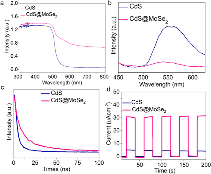
UV–vis measurements of CdS and CdS@MoSe2 heterojunctions were performed to analyze their optical properties, as shown in Fig. 2a. The light absorption edges of CdS and CdS@MoSe2 heterojunctions show slight differences, suggesting a shift in the bandgap (Eg) values of pure CdS and the CdS@MoSe2 composites. Notably, the composites exhibit enhanced absorption in the visible light region (520-700 nm) compared to pure CdS. This suggests that the introduction of MoSe2 modifies the inherent band structure of the CdS NRs, thereby improving their visible light absorption capacity through the formation of atomic-level chemical bonding interfaces. Photoluminescence (PL) analysis, which is commonly used to evaluate the efficiency of photogenerated electron transfer and recombination, was also performed on both CdS NRs and CdS@MoSe2 heterojunctions (Fig. 2b). The CdS@MoSe2 heterojunctions exhibited significantly weaker emission intensities (450–650 nm) than pure CdS under a 350 nm excitation wavelength, indicating more efficient separation of photogenerated electron-hole pairs between MoSe2 and CdS NRs under visible light. This behavior suggests a reduced probability of electron-hole recombination. The electron transfer between MoSe2 and CdS NRs suppresses the recombination of photogenerated electron-hole pairs, resulting in enhanced photocatalytic activity and stability for the CdS@MoSe2 heterojunctions. In Fig. 2c, the efficiency of photogenerated electron-hole pair separation in CdS@MoSe2 heterojunctions is shown to be much higher than in pure CdS NRs, implying that the efficient charge transfer between CdS and MoSe2 promotes an indirect recombination process in the CdS@MoSe2 compound. Fig. 2d presents the transient photocurrent response for the four samples. Under visible light irradiation, the CdS@MoSe2 heterojunctions display a higher transient photocurrent than pure CdS NRs, suggesting that the heterojunctions have a longer photogenerated charge carrier lifetime. The higher photocurrent of CdS@MoSe2 heterojunctions reflects the significant synergistic effect between CdS NRs and MoSe2 in enhancing the separation of electron-hole pairs generated by bandgap photoexcitation of CdS NRs under visible light.
Figure 2
Figure 2.
(a) The optical properties of CdS and CdS@MoSe2 heterojunctions were analyzed by UV−vis measurements. (b) PL of CdS and CdS@MoSe2 heterojunctions. (c) PL decay profiles of pure CdS and CdS@MoSe2. (d) Transient photocurrent responses pure CdS and CdS@MoSe2.
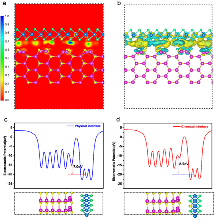
The interfacial alignment of energy bands, strongly influenced by the exposed facets of the components, plays a crucial role in determining the potential difference that drives interfacial charge transfer. Additionally, the electronic coupling and defect density at the interface, which depend on the compatibility of the facet structures, significantly affect the efficiency of charge transfer. Based on this, it can be concluded that highly efficient photocatalytic materials can be designed by optimizing both the exposed facets on the surface and the contact facets at the interface. To confirm this, we performed DFT calculations to explore the interlayer electronic interactions between CdS NRs and MoSe2. The results, including interfacial electron transfers and optimized atomic configurations of the hybrid, are shown in Fig. 3. Our calculations reveal that after MoSe2 is stacked onto CdS NRs, charge redistribution occurs due to electron transfer from CdS to MoSe2. This creates an electron-rich region on MoSe2 and a hole-rich region on the CdS sheet. The charge density is presented, with areas of high charge density shown in red. The overall charge density at the CdS/MoSe2 interface increases as a result of this electron transfer. The electron localization function (ELF) at the interface between CdS NRs and MoSe2 is as low as 0.1 (Fig. 3a), indicating a delocalized electron state at the interface. Fig. 3b provides a side view of the charge density difference in the CdS/MoSe2 hybrid, where yellow and green isosurfaces represent electron accumulation and depletion, respectively. As observed, the electron cloud density is distinctly localized between MoSe2 and MoSe2 doped with sulfur, clearly indicating strong bonding between Mo and S. Additionally, it is observed that the surface of MoSe2 is predominantly yellow, while the CdS NRs are primarily green, suggesting electron transfer from CdS NRs to MoSe2 across the intimate heterointerface. This transfer induces an internal electric field within the CdS/MoSe2 heterostructure. The work functions of the physical and chemical interfaces in the CdS/MoSe2 hybrid are shown in Figs. 3c and d. The difference in electrostatic potential between the physical and chemical interfaces of CdS/MoSe2 leads to charge redistribution. The electrostatic potential at the physical interface (7.0 eV) is much lower than that at the chemical interface (8.5 eV), indicating the formation of a built-in electric field at the chemical interface of CdS/MoSe2. Combining the experimental and theoretical results reveals the formation of a mesoscopic interface-driven composition with a unique electronic structure at the epitaxial CdS/MoSe2 interface. The well-aligned band structure of the CdS/MoSe2 hybrid is expected to minimize energy loss, thereby enhancing the charge transfer efficiency from CdS NRs to MoSe2 through the epitaxial interface.
Figure 3
Figure 3.
(a) Electron localization function of interfacial MoSe2 and CdS. (b) The side view of charge density difference of CdS/MoSe2 heterostructure. Yellow and green represent the charge accumulation and depletion regions, respectively. The work functions of CdS/MoSe2 with (c) physical interface and (d) chemical interface.
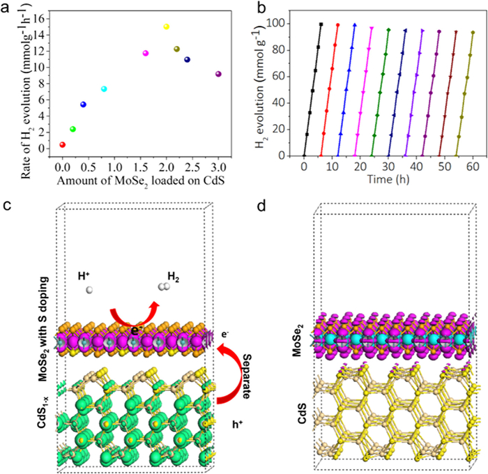
The pure CdS NR displayed insignificant catalytic activity, with a H2 evolution rate of 79.3 µmol h−1 g−1, due to the rapid recombination of electron-hole pairs within the CdS NRs. In contrast, the CdS@MoSe2 heterostructures demonstrate enhanced photocatalytic H2 production, attributed to the delayed recombination of electron-hole pairs by MoSe2 NSs. Notably, the CdS@MoSe2 heterostructures with 2 wt% MoSe2 NSs achieve the highest H2 production rate of 15 mmol h−1 g−1, approximately 56.9 times greater than that of pure CdS NRs (Fig. 4a). However, further increasing the MoSe2 cocatalyst loading leads to a reduction in the H2 evolution rate. This decline may be attributed to the high-density MoSe2 layers, which could obstruct the light absorption of CdS NRs. As shown in Table S1, CdS@MoSe2 represents a more efficient catalyst relative to other CdS based photocatalytic HER catalysts. Additionally, the photocatalytic stability of CdS@MoSe2 heterostructures with 2 wt% MoSe2 NSs was tested over four cycles (total of 60 h), as shown in Fig. 4b. After four cycles, no significant loss of activity was observed, indicating good stability for photocatalytic H2 evolution.
Figure 4
Figure 4.
(a) Average photocatalytic H2 evolution rate over CdS@MoSe2 heterojunctions loaded with different amount of MoSe2. (b) Repeated H2 evolution cycles catalyzed by CdS@MoSe2 heterojunctions under simulated solar light. All above measurements were performed under visible-light irradiation (λ ≥ 420 nm) in the mixed aqueous solution containing 0.35 mol/L Na2S and 0.25 mol/L Na2SO3 as sacrificial agents. Photocatalytic H2 evolution mechanism of CdS@MoSe2 heterojunctions with (c) chemical interface and (d) physical interface.
Electron-hole pairs are generated in semiconductors only when they absorb light of specific wavelengths, exciting the material with energy greater than its band gap. The separated electrons and holes are then transported from the interior of the semiconductor to its surface, where they migrate along the surface to the active sites. During this process, charge carriers may undergo recombination in both the bulk phase and during surface transport. Finally, the separated electrons and holes on the surface participate in the corresponding redox reactions at the active sites. The proposed photocatalytic HER mechanism is illustrated in Figs. 4c and d. Under simulated solar light illumination, the photogenerated electrons in CdS are efficiently transferred to MoSe2 monolayers via a strongly coupled interface as shown in Fig. S5 (Supporting information). The abundant hydrogen-evolving active sites in the few-layer MoSe2 allow CdS@MoSe2 heterojunctions with a chemical interface to achieve exceptionally high hydrogen evolution rates. The MoSe2 nanosheets, with low-coordination active sulfur atoms that strongly bond to H+ in the reaction solution, cover the hole surface of the shell of CdS@MoSe2 heterojunctions. These MoSe2 sheets can accept photogenerated electrons and serve as catalytic active sites for hydrogen evolution. MoSe2 is involved in different energy transfer mechanisms, which significantly enhances its photocatalytic activity. MoSe2 can be sensitized by CdS, forming a hybrid energy transfer architecture. The in-plane dipole moments of monolayer MoSe2 and CdS are strongly coupled. Nonradiative energy transfer from CdS to MoSe2 is enhanced by the reduced dielectric screening of the in-plane components of the donor dipole field. This generates more free electrons and holes, resulting in higher HER efficiencies [26-28]. As shown in Fig. 4d, only a physical interface is formed between CdS and MoSe2 when they are combined through physical mixing. The photogenerated electrons produced by CdS struggle to transfer to MoSe2 under illumination, limiting its catalytic performance. Furthermore, the CdS@MoSe2 displays a much smaller semicircle in Nyquist plots shown in Fig. S6 (Supporting information). These results verify that strong interfacial interaction could effectively facilitate charge separation and transfer in CdS@MoSe2, which contributes to an enhanced photocatalytic HER performance.
In this work, a novel 1D/2D heterostructure was constructed by growing MoSe2 nanosheets along the longitudinal axis of CdS nanorods through an anion exchange strategy. The strong interfacial coupling, enabled by well-matched crystal structures and strain-driven atomic substitution, plays a pivotal role in enhancing photocatalytic performance. This intimate interface facilitates efficient charge separation between the 1D CdS and 2D MoSe2 components, leading to a significantly improved hydrogen evolution rate of 15 mmol h-1 g-1 and an apparent quantum yield of 65% at 420 nm. Overall, this study presents a new route to engineer high-quality nanohybrid interfaces through strain-driven atomic substitution, offering promising prospects for advanced photocatalytic systems.
CRediT authorship contribution statement
Huimin Yue: Writing – original draft. Wenxiang Wang: Writing – original draft. Kun Wang: Data curation. Yongqi Liu: Data curation. Yang Liu: Data curation. Junan Pan: Data curation. Xia Liu: Writing – review & editing. Longlu Wang: Writing – review & editing.
Declaration of competing interest
The authors declare that they have no known competing financial interests or personal relationships that could have appeared to influence the work reported in this paper.
Acknowledgment
This work was financially supported by the Natural Science of China (No. 22206094).
Supplementary materials
Supplementary material associated with this article can be found, in the online version, at doi:10.1016/j.cclet.2025.111726.
[1]
X.H. Zhang, N. Li, J. Wu, et al., Appl. Catal. B: Environ. 229 (2018) 227–236. doi: 10.1016/j.apcatb.2018.02.025
Figure 1
SEM images of (a) pure CdS, (b) MoSe2 and (c) CdS@MoSe2 heterojunctions. (d-f) TEM images of CdS@MoSe2 heterojunctions (g) The FFT pattern taken at the circle in (d). (h) SAED pattern of CdS@MoSe2 heterojunctions. (i) Schematic model of the anion exchange. (j) HAADF-STEM and the corresponding STEM-EDS images of Cd, Mo, S and Se in CdS@MoSe2 heterojunctions with 5 wt% ratios of MoSe2.
Figure 2
(a) The optical properties of CdS and CdS@MoSe2 heterojunctions were analyzed by UV−vis measurements. (b) PL of CdS and CdS@MoSe2 heterojunctions. (c) PL decay profiles of pure CdS and CdS@MoSe2. (d) Transient photocurrent responses pure CdS and CdS@MoSe2.
Figure 3
(a) Electron localization function of interfacial MoSe2 and CdS. (b) The side view of charge density difference of CdS/MoSe2 heterostructure. Yellow and green represent the charge accumulation and depletion regions, respectively. The work functions of CdS/MoSe2 with (c) physical interface and (d) chemical interface.
Figure 4
(a) Average photocatalytic H2 evolution rate over CdS@MoSe2 heterojunctions loaded with different amount of MoSe2. (b) Repeated H2 evolution cycles catalyzed by CdS@MoSe2 heterojunctions under simulated solar light. All above measurements were performed under visible-light irradiation (λ ≥ 420 nm) in the mixed aqueous solution containing 0.35 mol/L Na2S and 0.25 mol/L Na2SO3 as sacrificial agents. Photocatalytic H2 evolution mechanism of CdS@MoSe2 heterojunctions with (c) chemical interface and (d) physical interface.


 DownLoad:

 下载:


 下载:

