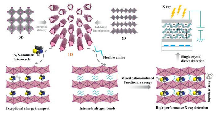
Scheme 1.
The design approach for 1D lead halide X-ray detection.
Exceptional one-dimensional hybrid lead halide for high-performance X-ray detection through hydrogen bond enhanced charge transport
Xue-Na Tang , Qingshun Fan , Guang-Ning Liu , Cuncheng Li , Zhihua Sun

The X-ray detection is extensively employed in multiple areas such as non-destructive product inspection, medical diagnostics, industrial production, and environmental monitoring [1–9]. In contrast to the indirect detection mechanism of entailing dual energy transformation stages in scintillators, the direct method of detecting X-ray radiation possesses the capability to instantaneously translate X-ray photons into electrical signals, theoretically manifesting superior sensitivity and refined spatial resolution. Over the years, traditional inorganic semiconductors such as crystalline Si, α-Se, and Cd(Zn)Te, have been dominating the market within the field of direct X-ray detection [10,11]. Nevertheless, the issues of high-energy consumption and small attenuation coefficients significantly hinder their further development. Consequently, developing new materials for advanced X-ray detectors is absolutely necessary.
Inorganic-organic hybrid lead halide perovskites (HLHPs) are highly attractive for radiation detection, because of their heavier average atomic mass, high mobility-lifetime (µτ) product, low-cost solution-based fabrication process and high resistivity [12–16]. At present, three-dimensional (3D) HLHP X-ray detectors based on single crystal CH3NH3PbBr3 and film CH3NH3PbI3 have been successfully fabricated and show excellent X-ray detection performances [17–19]. However, environmental stability and dark current drift (Idrift) seriously affect these detection devices, leading to material decomposition and performance degradation. Compared to the prototypical 3D HLHP, one-dimensional (1D) derivatives with large organic cations can improve moisture tolerance and effectively inhibit ion migration. In addition, combined with the advantages of low exciton dissociation and strong quantum confinement, 1D HLHPs possess notable photoelectric performance and operational stability [20–23]. For example, Liu et al. fabricated a UV photodetector based on 1D (DME)PbBr4 (DME = N,N’-dimethylethylenediamine) single crystals with remarkable photoresponsivity [24]. Zhang et al. obtained 1D (DMEDA)PbI4 (DMEDA = N,N’-dimethyl-1,2-ethanediamine) for UV–visible light detection, demonstrating excellent environmental stability [25]. However, the significant potential of 1D HLHPs in achieving high-performance X-ray detection remain largely unexplored [26,27]. Moreover, the majority of 1D perovskites tend to grow into needle-like crystals, which compromises their effectiveness as X-ray detectors due to issues such as reduced light absorption, increased scattering, and difficulties in fabricating planar devices [28]. Therefore, design and synthesis of large-area, high-performance 1D HLHP single crystal for X-ray detection is urgent and challenging.
In this work, we propose the “mixed cation-induced functional synergy” strategy (Scheme 1), which involves incorporating aromatic thiazol-2-aminium cation (ATZ)+ with aliphatic ethanaminium cation (EA)+ to assemble a 1D HLHP, namely (ATZ)(EA)4Pb3I11 (1). Therein, thiazole derivatives possess loose valence π electrons that contribute to their exceptional charge transport ability [29–32]. Meanwhile, the incorporation of aliphatic ammonium cation forms intense hydrogen bonds that facilitate large size crystal growth. The H···I type hydrogen bonds in 1 account for 69.7% of the total Hirshfeld surface, which is larger than those of HLHPs containing solely (ATZ)+ or (EA)+ cations. Due to these structural features, the single crystals of 1 show enhanced environmental stability and remarkable semiconducting properties such as a high resistivity of 1.94 × 10¹¹ Ω cm and a µτ product as large as 2.22 × 10⁻⁴ cm2/V. All these intrinsic attributes enable the single crystal of 1 to show high-performance X-ray detection with a high X-ray detection sensitivity of 1356 µC Gyair−1 cm−2 at 33.3 V/mm and an ultra-low Idrift of 5.01 × 10⁻⁸ nA cm−1 s−1 V−1.
High-quality yellow crystals of 1 with dimensions of 9 × 3 × 2 mm3 were achieved by gradually cooling the HI solution containing lead acetate, 2-aminothiazole and ethylamine (Fig. 1a, for details see Supporting information). Single crystal X-ray diffraction (XRD) indicates that 1 crystallizes in the centrosymmetric space group Cmcm (No. 63) with an orthorhombic structure (Table S1 in Supporting information). The crystal is composed of three structural moieties: One (ATZ)+ cation, four (EA)+ cations and an infinite anionic chain (Fig. 1b and Fig. S1 in Supporting information). Each Pb atom is in a six-coordinated (PbI6) octahedral environment. Three (PbI6) octahedra share faces to connect into a linear trinuclear unit, which further enjoys the terminal I atoms with the neighboring unit to give a zigzag infinite anionic chain along the c axis (Fig. 1c and Fig. S2 in Supporting information). The anionic framework represents a rarely reported chain-like structure, which is different from the 2D layer with the same Pb and I compositions but with different connections of (PbI6) octahedra (Fig. S3 in Supporting information) [33]. It also differs from the chains formed by edge-sharing (PbI6) in the two closely related HLHPs (EA)PbI3 and (ATZ)PbI3 (Figs. S4-S7 in Supporting information). The Pb–I bond distances span from 3.1554(9) Å to 3.2794(9) Å, and the I–Pb–I bond angles span from 84.34(3)° to 180.0°, all within expected values (Table S2 in Supporting information) [34]. The ΔR parameter defined by Brown was employed to assess the distortions of the (PbI6) octahedra (Table S3 in Supporting information) [35]. The (Pb2I6) unit located at the terminal of the trinuclear unit with an ΔR value of 3.6 × 10⁻³ is larger than the value of 2.1 × 10⁻⁴ for (Pb1I6), which indicates Pb2 occupies a more severe distorted coordination geometry.
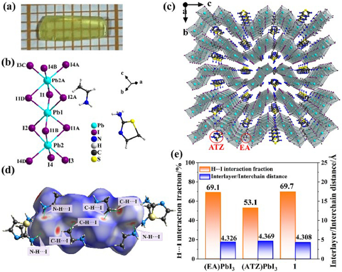
The (ATZ)+ and the (EA)+ cations are arranged in an orderly staggered arrangement between anionic chains, with the 3D packing diagram shown in Fig. S8 (Supporting information). Necessary restraints on the distances and angles of the mixed cation were used following the geometry of such molecules [33]. Further analysis of the structure reveals that the minimum distance between H and I is 2.758 Å, which is shorter than the van der Waals (vdW) radii summation (3.08 Å). This suggests the existence of hydrogen bond interactions between the mixed cations and inorganic chain (Table S4 in Supporting information).
The Hirshfeld surface analysis was performed to examine the non-covalent interactions in 1 (Fig. 1d). Different colors on the dnorm surface correspond to different contact distances separating the neighboring atoms. The red color indicates the contact distance shorter than sum of VdW radii, suggesting the presence of hydrogen bonds. The white color indicates that the distance approaches the sum of vdW radii. Blue color illustrates the distance is longer than vdW separation, too far for interaction [36]. Herein, the large red spots in the dnorm surface of 1 correspond to the strong N/C–H···I hydrogen bonds between flexible (EA)+ spacer and inorganic anionic chain. The red to white spots are attributed to the N–H···I hydrogen bonds between aromatic (ATZ)+ spacers and anionic chain. These results are in accord with the crystallographic hydrogen bond analyses and confirm that the alkyl ammonium cation is more favorable to form strong hydrogen bonds (Table S4). The 2D fingerprint plot was analyzed to highlight particular atom pair contacts (Fig. S9 in Supporting information). The region corresponding to the N/C–H···I hydrogen bond comprises 69.7% of the total Hirshfeld surface, which is larger than (EA)PbI3 (62.0%) and (ATZ)PbI3 (53.1%) (Figs. S10 and S11 in Supporting information). The intense hydrogen bonds in 1 bring about the minimum interchain distance of 4.308 Å, which is smaller than the interchain distances in (ATZ)PbI3 (4.369 Å) and (EA)PbI3 (4.326 Å) (Fig. 1e, Figs. S12 and S13, Table S5 in Supporting information). All the structural features facilitate the charge transport in 1.
To assess the semiconducting characteristics of 1, we conducted UV–vis diffuse reflection spectroscopy measurements. As depicted in Fig. 2a, the absorption spectrum of 1 shows a clear and distinct absorption edge positioned at 627 nm, devoid of any additional notable absorption feature. The Tauc equation yields an optical band gap (Eg) of 2.20 eV. To determine the electronic structure, the ultraviolet photoelectron spectroscopy (UPS) measurement was conducted for 1. The Fermi energy level (EF) is calculated as −3.67 eV according to the work function (
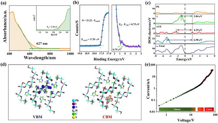
The computation of electronic band structures and the total and partial density of states (DOSs) was performed utilizing the density functional theory (DFT) method. The calculated band structure of 1 is depicted in Fig. S15 (Supporting information), revealing an indirect band gap feature with a theoretical band gap value of 2.13 eV [38,39]. The total and partial DOS plots analyses reveal that the valence band maximum (VBM) are mainly attributed to the 5p state of iodine and the conduction band minimum (CBM) are mainly attributed to the p-π* antibonding orbitals of (ATZ)+ cation, indicating that both the inorganic chain and the aromatic (ATZ)+ cation are primarily responsible for the photon-induced charge transfer in 1 (Figs. 2c and d). The (ATZ)+ cation has a smaller molecular energy gap (~4.29 eV), which brings the p-π and p-π* orbitals closer to the band edges, both in the VBM and CBM, compared to the
Space-charge-limited current (SCLC) measurement was employed to determine the carrier mobility (µ) value of 1. The current-voltage plot of the Ag/1/Ag sandwich device exhibit three distinct regions: The low-voltage Ohmic region (first power law), the high-voltage Child region (second power law), and the trap-filled limited (TFL) region between these two regions (Fig. 2e). Fitting the Child region with the Mott–Gurney law equation [41]:
|
|
(1) |
where J denotes the current density, L denotes the thickness of the sample (1.5 mm), ε is the dielectric constant (with an average values of 18.6, Fig. S19 in Supporting information), and V is the bias voltage [42–44], gives the µ value of 1 as 0.32 cm2 V−1 s−1; this value is slightly lower than the classic FAPbI3 of 4.4 cm2 V−1 s−1, FA = HC(NH2)2+ [45].
The exciton binding energy (Eb), was obtained through a temperature-dependent photoluminescence technique [46,47]. As shown in Figs. S20 and S21 (Supporting information), 1 shows photoluminescence under 110 K and emits stronger with the temperature lowered to 77 K. The Arrhenius function fitting of the intensity versus 1/T plot afford an Eb value of 40 meV, which is close to the values for MAPbI3 (45 meV) and FAPbI3 (35 meV), this proves 1 has good electron-hole separation, implying the X-ray detection potential for 1 [48,49].
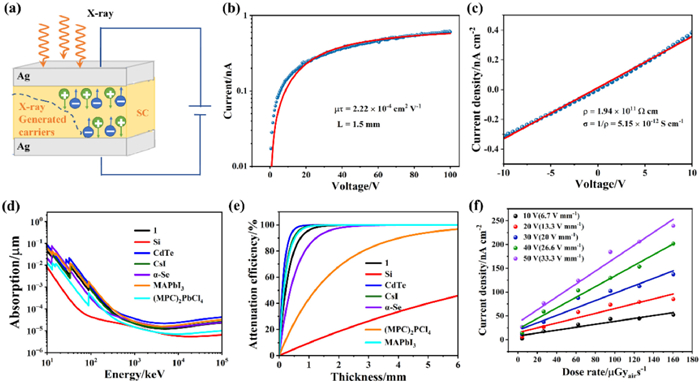
To assess charge collecting capacity under X-ray irradiation, a vertical-type detector utilizing the single crystal of 1 was fabricated with electrode area of 0.2 mm2 and thickness of 1.5 mm (Fig. 3a). To achieve high sensitivity and low detection limits in X-ray detection, a high µτ product and large resistivity are indispensable key factors [2].
The
|
|
(2) |
The symbols I0, V, and L are used to denote the saturated photocurrent, the applied bias, and the crystal thickness respectively. As shown in Fig. 3b, the
To gauge the potential of single crystal for X-ray detection, we calculated the absorption coefficient of the single crystals with the variation of photon energy. Fig. 3d clearly shows that the absorption coefficient of 1 is greater than Si, and it aligns closely with those of CdTe, CsI, α-Se, MAPbI3 and (MPC)2PbI4 (MPC = 6-mercaptopyridine-3-carboxylic acid) in the energy range of 10–104 keV [55]. As shown in Fig. 3e, upon attaining a thickness of 1.5 mm for the single crystal of 1, the attenuation rate for 50 keV X-ray photons nearly attains 100% effectiveness. The exceptional X-ray absorption capability of 1 inspires us to quantify its reactivity towards X-ray photons.
As shown in Fig. S22 (Supporting information), the electrical responses of the single-crystal detector under variable X-ray radiation were recorded with an electric field of 10 V, and intense photocurrent responses were detected under even a small difference in dose rates. Sensitivity (S) represents a crucial performance indicator for direct X-ray detectors, reflecting the capacity of an X-ray detector to respond to a unit dose rate applied over a unit area. It can be determined using the subsequent formula [50]:
|
|
(3) |
where Iph is the photocurrent, D is the dose rate and A is the active area of a device. The X-ray response current density at different dose rates and electric fields was used to calculate the sensitivity (Fig. 3f). As the bias voltage raised from 10 V to 50 V (electric field increasing from 6.7 V/mm to 33.3 V/mm), the sensitivities determined utilizing the gradient of the linear regression, showed a marked increase from 307 µC Gyair−1 cm−2 to 1356 µC Gyair−1 cm−2 (Fig. S23 in Supporting information). The value at 50 V (33.3 V/mm) is second to the highest 1D fully inorganic lead-based X-ray detector CsPbI3, and even exceeds most 2D single crystal detectors (Table S6 in Supporting information). As a result, 1 exhibits a high sensitivity at relatively low electric field. The performance of single crystal 1 in detecting X-rays supports its potential application in the medical field, where lower doses of X-rays contribute to increased safety in medical diagnostics. Furthermore, the detection limit is a pivotal metric for X-ray detectors, being inherently influenced by the signal-to-noise ratio (SNR, see formula in Supporting information). The SNRs of the response current were computed across various dose rates, and the dependence of SNR on the dose rate is graphically illustrated in Fig. S24 (Supporting information). The device demonstrates a remarkable photoelectric response, with a detection limit of 4.3 μGyair/s at an SNR of 5. This value is lower than the 5.5 µGyair/s required for conventional medical diagnosis, indicating potential applications of 1 in medical examinations.
In addition, the response time (τ) of X-ray detector was evaluated by analyzing the “on/off” switching cycle plot depicted in Fig. S25 (Supporting information). The rise and decay times are determined as 280 and 570 ms, which represent the times for photocurrent to rise to 90% from 10% and fall to 10% from 90%. Such a short response time implies the promising radiographic application of 1.
The irradiation stability of the X-ray detector was also evaluated. The dark current of the X-ray detector displays only subtle differences in the duration of ~600 s under a bias of 10 V (Fig. 4a). In general, a low Idrift could reduce the dark current noise signal and improves the SNR. Then, the Idrift was calculated using the following formula [56]:
|
|
(4) |
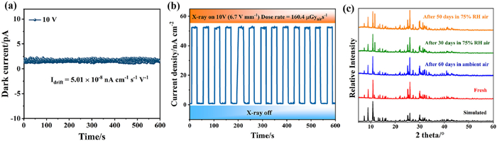
where J0 denotes the dark current density at the beginning, Jt represents the dark current density at test time t, E represents the applied electric field. The Idrift of the X-ray detector is 5.01 × 10⁻⁸ nA cm−1 s−1 V−1 at 6.7 V/mm. This value falls below most previously reported 2D HLHP single crystal X-ray detectors, for example, (DGA)PbI4 with a value of 5.97 × 10⁻⁶ nA cm−1 s−1 V−1 at 2000 V/mm and (PEA)2PbI4 with a value of 1.90 × 10⁻⁷ nA cm−1 s−1 V−1 at 4545 V/mm (for more comparison, see Table S7 in Supporting information). It suggests that the Idrift within the X-ray detector of 1 is insignificant, and the ion migration is effectively suppressed within the single crystal.
The current density versus time plot shown in Fig. S26 (Supporting information) indicates that the photocurrent kept stable without significant attenuation under an uninterrupted X-ray bombardment with a dose rate of 160.4 μGyair/s for at least 600 s. Further, the photocurrent shows no obvious changes under repeated cycles of “on/off” X-ray irradiation with a constant bias electric field of 10 V, which suggests the outstanding photoelectric stability of the single crystal detector of 1 (Fig. 4b).
The elemental analysis and infrared spectrum analysis correspond well to the structural data (Table S8 and Fig. S27 in Supporting information). The purity of the phase composition within the collected single crystals of 1 was confirmed through the utilization of powder X-ray diffraction (PXRD) analysis. The observed diffraction peaks closely match the calculated diffraction peaks derived from the structural data (Fig. 4c). These results prove the high single-phase purity nature and facilitate the application of the single crystal of 1 in the field of direct X-ray detection [57]. Thermogravimetric analysis for 1 confirms the excellent thermal stability, which can remain stable up to 509 K (Fig. S28 in Supporting information). Considering the intense hydrogen bonds in 1, the endurance of the single crystals in moisture air was evaluated. As shown in Fig. 4c, Figs. S29 and S30 (Supporting information), 1 remains structure robust without any visible change in 75% relative humidity (RH) air for at least 50 days, which is significantly longer than the values of 7 and 3 days for (ATZ)PbI3 and (EA)PbI3, respectively. These results confirm the (ATZ)+ alloyed mixed cationic spacer in enhancing the stability of 1D HLHPs.
We prepared a new 1D HLHP of 1 with the formula of (ATZ)(EA)4Pb3I11, which contains an 1D zigzag anionic chain, being different from chains with either (ATZ)+ or (EA)+ as the sole cation. The proposed mixed cation strategy induces intense hydrogen bonds accounting for 69.7% of the total Hirshfeld surface, which promotes growth of large single crystals and significantly enhances the environmental stability of 1. Moreover, the single crystal of 1 boasts an ultra-low Idrift of 5.01 × 10⁻⁸ nA cm−1 s−1 V−1 and an impressive sensitivity of 1356 µC Gyair−1 cm−2 at 33.3 V/mm, owing to its high resistivity and substantial µτ product, making it ideal for X-ray direct detection. The single crystal of 1 represents a rare example of 1D HLHP for X-ray detection. The research presents a new frontier and a broad range of possibilities for the application of 1D HLHPs in the realm of X-ray detection.
The authors declare that they have no known competing financial interests or personal relationships that could have appeared to influence the work reported in this paper.
Xue-Na Tang: Writing – original draft, Investigation, Data curation. Qingshun Fan: Writing – original draft, Visualization, Methodology. Guang-Ning Liu: Writing – review & editing, Methodology, Funding acquisition, Formal analysis. Cuncheng Li: Writing – review & editing, Supervision, Funding acquisition, Project administration. Zhihua Sun: Writing – review & editing, Supervision, Funding acquisition.
This work was supported by the Natural Science Foundation of Shandong Province (No. ZR2024MB006), Jinan Research Leader's Studio (No. 2019GXRC053), the Natural Science Foundation of China (Nos. 22125110, 21833010, 22075285, 52202194), Fujian Science & Technology Innovation Laboratory for Optoelectronic Information of China (No. 2021ZR126), the Key Research Program of Frontier Sciences of CAS (No. ZDBS-LY-SLH024), Strategic Priority Research Program of CAS (No. XDB20010200) and the Natural Science Foundation of Fujian Province (No. 2023J02028).
Supplementary material associated with this article can be found, in the online version, at doi:
Y. Hassan, J.H. Park, M.L. Crawford, et al., Nature 591 (2021) 72–77. doi: 10.1038/s41586-021-03217-8
M. Chen, X. Dong, D. Chu, et al., Adv. Mater. 35 (2023) 2211977. doi: 10.1002/adma.202211977
Y.C. Kim, K.H. Kim, D.Y. Son, et al., Nature 550 (2017) 87–91. doi: 10.1038/nature24032
R. Rahman, A.J. Plater, P.J. Nolan, et al., Radiat. Prot. Dosim. 154 (2012) 477–482. doi: 10.1007/s10509-012-1114-6
S. Tie, W. Zhao, W. Huang, et al., J. Phys. Chem. Lett. 11 (2020) 7939–7945. doi: 10.1021/acs.jpclett.0c02343
H. Wei, Y. Fang, P. Mulligan, et al., Nat. Photonics 10 (2016) 333–339. doi: 10.1038/nphoton.2016.41
H. Wei, J. Huang, Nat. Commun. 10 (2019) 1066. doi: 10.1038/s41467-019-08981-w
H. Wu, Y. Ge, G. Niu, et al., Matter 4 (2021) 144–163. doi: 10.1016/j.matt.2020.11.015
Y. Zhou, J. Chen, O.M. Bakr, et al., ACS Energy Lett. 6 (2021) 739–768. doi: 10.1021/acsenergylett.0c02430
Y. Liu, Y. Zhang, X. Zhu, et al., Adv. Mater. 33 (2021) 2006010. doi: 10.1002/adma.202006010
J. Kim, D.W. Kim, S.H. Kim, et al., J. Instrum. 12 (2017) C01029. doi: 10.1088/1748-0221/12/01/C01029
A. Jana, S. Cho, S.A. Patil, et al., Mater. Today 55 (2022) 110–136. doi: 10.1016/j.mattod.2022.04.009
P. Wangyang, C. Gong, G. Rao, et al., Adv. Opt. Mater. 6 (2018) 1701302. doi: 10.1002/adom.201701302
S. Yakunin, D.N. Dirin, Y. Shynkarenko, et al., Nat. Photon. 10 (2016) 585–589. doi: 10.1038/nphoton.2016.139
Z. Zhang, J. Jin, Y. Lin, et al., Angew. Chem. Int. Ed. 63 (2024) e202400760. doi: 10.1002/anie.202400760
Y. Ge, Q. Wang, F. Yang, et al., Inorg. Chem. 60 (2021) 8322–8330. doi: 10.1021/acs.inorgchem.1c01037
Y. Wu, J. Feng, Z. Yang, et al., Adv. Sci. 10 (2022) 2205536.
X. Liu, J. Ren, Y.A. Chen, et al., Sci. China Inf. Sci. 67 (2024) 131401. doi: 10.1007/s11432-023-3856-4
T. Zhu, X. Gong, InfoMat 3 (2021) 1039–1069. doi: 10.1002/inf2.12211
Y. Lin, Y. Bai, Y. Fang, et al., ACS Energy Lett. 2 (2017) 1571–1572. doi: 10.1021/acsenergylett.7b00442
C. Zhou, H. Lin, Q. He, et al., Mater. Sci. Eng. R Rep. 137 (2019) 38–65. doi: 10.1016/j.mser.2018.12.001
J.Y. Liu, M.M. Lun, Z.J. Wang, et al., Chem. Sci. 15 (2024) 16612–16617. doi: 10.1039/d4sc03571b
H. Xu, Z. Zhang, X. Dong, et al., Inorg. Chem. 61 (2022) 4752–4759. doi: 10.1021/acs.inorgchem.2c00169
T. Liu, W. Tang, S. Luong, et al., Nanoscale 12 (2020) 9688–9695. doi: 10.1039/d0nr01495h
Y. Zhang, F. Liu, C. Jiang, et al., J. Mater. Chem. C 9 (2021) 3470–3476. doi: 10.1039/d0tc05983h
J.H.Y.J. Wang, J. Chen, S.H. Wang, Chem. Commun. 60 (2024) 3311. doi: 10.1039/d4cc00510d
D.L. Hu, J.Y. Guo, M.J. Xie, et al., ACS Mater. Lett. 6 (2024) 4841–4846. doi: 10.1021/acsmaterialslett.4c01753
K.R. Dudipala, T.H. Le, W. Nie, et al., Adv. Mater. 36 (2023) 2304523.
C. Ma, L. Gao, Z. Xu, et al., Chem. Mater. 34 (2022) 1699–1709. doi: 10.1021/acs.chemmater.1c03832
Z. Xu, D. Lu, X. Dong, et al., Adv. Mater. 33 (2021) e2105083. doi: 10.1002/adma.202105083
X. Li, W. Ke, B. Traoré, et al., J. Am. Chem. Soc. 141 (2019) 12880–12890. doi: 10.1021/jacs.9b06398
Q. Sun, M.H. Shang, Z. Fang, et al., Small 19 (2023) e2207755. doi: 10.1002/smll.202207755
M. Ben Haj Salah, N. Mercier, M. Allain, et al., Chem. Mater. 34 (2022) 5780–5790. doi: 10.1021/acs.chemmater.2c00130
J.W. Li, C.C. Jiang, Chin. J. Struct. Chem. 37 (2018) 1635.
I.D. Brown, Acta Crystallogr. Sect. B: Struct. Sci. 62 (2006) 692–694. doi: 10.1107/S010876810601322X
A.V. Parwani, CrystEngComm 11 (2009) 19–32.
G.N. Liu, X.N. Tang, J.S. Guo, et al., Sens. Actuator B: Chem. 399 (2024) 134864.
L. Lu, Y. Ma, J. Wang, et al., Chemistry 27 (2021) 9267–9271. doi: 10.1002/chem.202100691
R.W. Godby, M. Schlüter, L.J. Sham, Phys. Rev. B 36 (1987) 6497–6500.
C. Ni, Y. Huang, T. Zeng, et al., Angew. Chem. Int. Ed. 59 (2020) 13977–13983. doi: 10.1002/anie.202006112
P.N. Murgatroyd, J. Phys. D: Appl. Phys. 3 (1970), doi: 10.1088/0022-3727/3/2/308.
W. Pan, H. Wu, J. Luo, et al., Nat. Photon. 11 (2017) 726–732. doi: 10.1038/s41566-017-0012-4
S. Han, Y. Ma, L. Hua, et al., J. Am. Chem. Soc. 144 (2022) 20315–20322. doi: 10.1021/jacs.2c07892
Y. Ma, W. Guo, Q. Fan, et al., Adv. Funct. Mater. 33 (2023) 2210235.
Q. Han, S.H. Bae, P. Sun, et al., Adv. Mater. 28 (2016) 2253–2258. doi: 10.1002/adma.201505002
W.Q. Liao, Y.Y. Tang, P.F. Li, et al., J. Am. Chem. Soc. 140 (2018) 3975–3980. doi: 10.1021/jacs.7b12524
G.N. Liu, R.D. Xu, M.K. Li, et al., Chem. Commun. 58 (2022) 2858–2861. doi: 10.1039/d2cc00145d
T. Ishihara, J. Lumin. 60 (1994) 269–274.
A. Miyata, A. Mitioglu, P. Plochocka, et al., Nat. Phys. 11 (2015) 582–587. doi: 10.1038/nphys3357
Y. Liu, Z. Xu, Z. Yang, et al., Matter 3 (2020) 180–196.
Q. Fan, H. Xu, S. You, et al., Small 19 (2023) 2301594.
K. Tao, Y. Li, C. Ji, et al., Chem. Mater. 31 (2019) 5927–5932. doi: 10.1021/acs.chemmater.9b02263
Z.K. Zhu, T. Zhu, J. Wu, et al., Adv. Funct. Mater. 33 (2023) 2214660.
T. Zhu, W. Weng, C. Ji, et al., J. Am. Chem. Soc. 144 (2022) 18062–18068. doi: 10.1021/jacs.2c07891
D. Kowal, M. Makowski, M.E. Witkowski, et al., Mater. Today Chem. 29 (2023) 101455.
Q. Fan, Y. Ma, S. You, et al., Adv. Funct. Mater. 34 (2024) 2312395.
Q. Chen, J. Wu, X. Ou, et al., Nature 561 (2018) 88–93. doi: 10.1038/s41586-018-0451-1

Figure 1 (a) Solution-grown bulk crystal of 1. (b) Molecular structure of 1. (c) 3D packing diagram seen along the a axis direction. (d) View of the dnorm mapped on the Hirshfeld surface of trinuclear building unit. (e) Interlayer or interchain distances and the fractions of H···I contact in 1, (EA)PbI3 and (ATZ)PbI3.

Figure 2 (a) Absorption spectrum of 1. Inset: the deduced band gap. (b) Secondary electron cut off measured with He I (left), valence band for the Fermi level (right). (c) Total and partial DOSs of 1. Energy gaps corresponding to possible charge transfer are labeled. (d) Spatial plots of VBM and CBM orbitals, respectively. (e) Logarithmic I-V plot based on the SCLC method.

Figure 3 (a) Schematic illustration of the detector structure made from a single crystal. (b) Photoconductivity measurement of the single crystal device. (c) Bulk resistivity and conductivity measurement. (d) Calculated absorption spectra of 1, crystalline Si, CdTe, CsI, α-Se, MAPbI3 and (MPC)2PbI4. (e) Attenuation efficiency of 50 keV X-ray photons under different crystal thicknesses for 1, Si, CdTe, CsI, α-Se, (MPC)2PbI4 and MAPbI3. (f) Dose-rate-dependent response current density at various electric fields.

 扫一扫看文章

扫一扫关注我们
 DownLoad:

 下载:
下载:

 下载:
下载: