Figure 1.
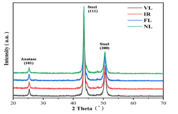
XRD pattern of the as-grown films

As a well-established technology to grow high quality films, magnetron sputtering has now been applied in many industries including solar cells, sensor, thin film transistor (TFT), optical lens, circuits, light-emitting diode (LED), etc[1-4]. Particularly, sputtering has the advantage of low temperature deposition which can be used to deposit lots of inorganic element and compounds on various substrate such as glass, ceramics, metals, textiles and flexible polymer substrate[5, 6].
The development of magnetron sputtering technique experiences several stages. From the classical planar magnetron sputtering, inductively coupled plasma source magnetron sputtering, microwave amplified magnetron sputtering and high power impulse magnetron sputtering, both of them focus on the modification of the flux of ions sputtering from the target[7-10]. Photo-assisted growth methods have been studied since 1980s[11]. Most photoassisted growth methods are metal-organic chemical vapor deposition (MOCVD), sol-gel in which the react species are organic compounds[12]. The photo is induced to activate or decompose the react species[13]. Fujita et al reduced the growth temperature of ZnSe from 500 to 300 ℃ by photo assisted MOCVD to reduce the defects in the ZnSe epilayers[14]. Li et al. improved the quality ZnO films due to the ethyl radical releasing from the metal atom, thus leading to incorporation into the lattice[15]. However, it is lack of knowledge about the affection of photo on the film's growth for magnetron sputtering.
In this work, we induce a photo-assisted magnetron sputtering method to improve the quality of as-grown titanium dioxide film. The influence of incident light on the photocatalytic activity has been studied. And the mechanism of photo-assisted growth has been discussed.
TiO2 thin films are deposited on stainless steel substrates (2cm × 2cm) by sputtered titanium target. During the sputtering process, the working gas is a mixture of Ar (99.999% pure) and O2 (99.99% pure), and the base vacuum is 3 × 10⁻⁵ Pa. For all the samples, the sputtering power, total working pressure, Ar flow rate and O2 flow rate are set to 140 W, 2.0 Pa, 14 sccm (standard cubic centimeter per minute) and 6 sccm, respectively. The incident light is provided by a 300 W Xenon lamp (PLSSXE300C). The as-prepared samples are labelled as FL, VL, IR and NL for deposition under light with full spectrum, light filtered with UV-cutoff filter (λ≥S420 nm) and light filtered with UV-vis cutoff filter (λ ≥ 600 nm) and without light respectively.
Crystallinity of the films is determined by Rikagu Miniflex 600 X-ray diffraction. Electron microscope analysis is carried on a JEOLJSM-6700F Scanning electronic microscopy (SEM). The transmittance spectra of the films are obtained via the Shimadzu UV-2500 UV/Vis Spectrometer. The photoelectrochemical measurements of the as-prepared samples are also performed in 4% formaldehyde aqueous solution with 0.1 M K2SO4 to increase the conductivity of the solution. All electrochemical measurements are conducted on a CHI 660D electrochemical workstation, using a three-electrode test cell. Transient absorption Spectra are obtained by an ultrafast HELIOS Femtosecond Transient Absorption Spectrometer. XPS measurements are performed in a Thermo Fisher K-Alpha+ system with an AlKα source.
The simulated sunlight is provided by a xenon source lamp. The photocatalytic H2 evolution test is conducted in an online photocatalytic hydrogen production system. A xenon arc lamp (Perfect Light PLS-SXE300) is used as a light source and positioned 20 cm away from the film. The sample fixed on bracket made of PTFE is dipped in 100 mL formaldehyde aqueous solution (4%) using a magnetic stirrer. And the hydrogen is analyzed by an online gas chromatograph (GC-2014, Shimadzu) which is equipped with a TCD detector and a packed column (carbon molecular sieve) using Argon (99.999%) as the carrier gas.
Fig. 1 shows the XRD pattern of as-grown films. There are only three diffraction peaks listed in the XRD pattern. Except two peaks attributed to the substrate, all films exhibit anatase (101) preferred orientation which is in accordance with our previous study[16]. While inducing light during film growth, the peak intensity of anatase (101) increases. It indicates that the crystallinity of the films is improved with photo assistance.
The surface morphology is analyzed by AFM. As shown in Fig. 2, the films show a typical island growth pattern. The surface morphology of the films doesn't show a remarkable change for depositing with or without photo-assistance. To analyze the microstructure of the films, SEM and TEM tests are carried out and shown in Figs. 3 and 4. SEM images of the films show a columnar structure pattern. Corresponding to island growth pattern observed in AFM, the particle coalescence phenomenon is clearly observed. It is known that the crystal structure of TiO2 belongs to tetragonal system with space group I41/amd, while the steel substrate is of cubic system in space group Fm3m. The films show a typical Volmer-Weber growth mode due to the low substrate temperature and lattice mismatch. TEM image in Fig. 4 clearly shows lattice fringes and the observed lattice fringes of all samples have d-spacing of 0.35 nm, which is in accordance with d (101) of anatase TiO2. TEM images suggest an anatase structure of the films, which is consistent with the XRD results. The morphology and structure of the films remain unchanged, indicating that the film growth is independent to the incident light.
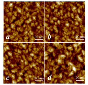
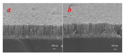
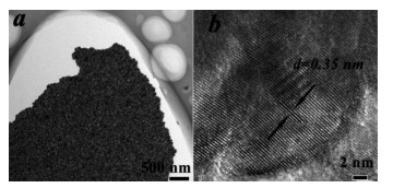
Fig. 5 shows UV-vis absorption spectra of the TiO2 films prepared on the glass substrate. All films exhibit the same absorption edge and spectral interference, indicating the same film thickness and refractive index[17, 18]. Fig. 6 shows the reflectance spectra of TiO2 prepared on the steel substrates. The steel substrate possesses high reflectance rate. After being coated with TiO2 films, the reflectance decreases significantly. Consistent with the transmittance spectra, all films show the same spectral interference. The similar spectral interference indicates the film is uniform and homogeneous with the consistent film thickness which is ideal for comparative study on the photocatalytic performance.
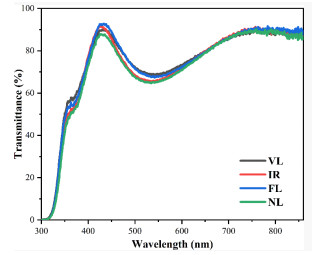
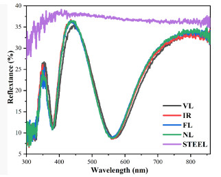
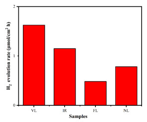
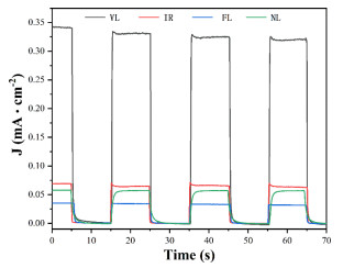
Fig. 7 shows the photocatalytic H2 evolution rate as the function of the wavelength of the incident photon. Interestingly, the photocatalytic performance is changed while the morphology and optical properties of the films remain the same. The photocatalytic performance of the film is improved for deposition under infrared light and further enhanced for deposition under visible light. However, the performance reduces while depositing under full spectrum lighting. Electrochemical measurement also shows the different behaviors of the films. The photocurrent response is carried out to analyze the efficient charge separation during photocatalytic activity. As shown in Fig. 8, all films exhibit stable photocurrent response. The photocurrent density increases sharply under each irradiation and recovers rapidly in the dark. The reproducibility of the photocurrent indicates the stability of photocatalytic activity of the films. Compared with NL, the photocurrent density of the photo-assisted deposited films increases for sample VL and drops dramatically for sample FL. Consistent with the photocatalytic H2 evolution activity, the results reveal the notable difference in the photocatalytic performance of the films which are dependent to the incident light during photo-assisted deposition.
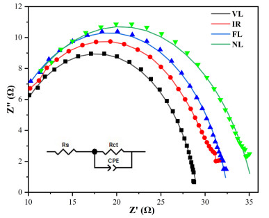
We have previously demonstrated that the defects in TiO2 thin films could be tuned by the incident photons during sputtering. We now focus on the effects of defects on the photocatalytic activity of TiO2. It is known that defects in TiO2 such as Ti3+ are beneficial for the utilization of visual light[19, 20]. And the hydrogen evolution rate of TiO2 nanoparticles grown under 254 nm UV lamp is 3.7 fold compared to that of the normal TiO2[21]. However, we observe a decrease of photocatalytic activity of sample FL. To verify the different behaviors during photocatalytic activity, the electrochemical impedance spectroscopy (EIS) is employed to analyze the carrier transferring mechanism. Fig. 9 shows the Nyquist plots of the impedance data. VL possesses small capacitive arcs, showing that it has higher efficiency in transferring the carriers. The single capacitive arcs are modeled by the simple equivalent circuit (Fig. 9), consisting of a resistor Rs in series with a resistor Rct and capacitor CPE in parallel, where Rct and CPE represent the charge transfer resistance and the double layer capacitance, respectively. As shown in Table 1, the Rct of FL is higher than that of VL, suggesting the low efficiency in the transferring of photo-generated carriers.
 DownLoad:
CSV
DownLoad:
CSV
| Rs (Ω) | Rct (Ω) | CPE (F) | |
| NL | 5.24 | 30.44 | 4.23 × 10⁻⁷ |
| VL | 6.26 | 22.88 | 2.16 × 10⁻⁷ |
| IR | 5.20 | 26.77 | 4.32 × 10⁻⁷ |
| FL | 5.58 | 27.08 | 2.40 × 10⁻⁷ |
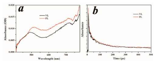
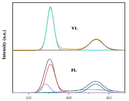
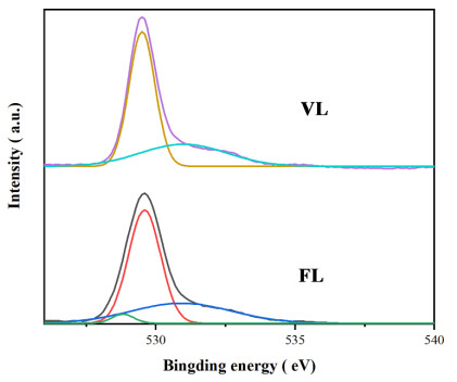
To clarify the impact of the defects induced by UV light on the kinetics of the carriers in TiO2, transient absorption spectra are employed to study the carrier behaviors under excitation. In Fig. 10, the absorption peaks of trapped electrons and holes are clearly shown in the spectra[22, 23]. The similar spectrum and lifetime of the trapped state in FL and VL indicate the same type of trapped state in the two samples. FL has much higher absorption peaks than VL, which means the concentration of the trapped states of FL is higher than that of VL. It is known that the trapped states would significantly reduce the carrier mobility and lifetime. The different behaviors of the carrier under excitation in the films which are consistent with the EIS spectra clearly show the influence of defects on the transferring efficiency of the carriers. To study the trapped states in the films, XPS survey are conducted. Fig. 11 shows the Ti 2p spectra of FL and VL. Compared with VL, the Ti 2p spectrum in FL is slightly broadened and exhibits a tail in the region of lower binding energy. It is known that the Ti3+ has a lower binding energy than Ti4+, which would result in the shift of peak. The O 1s XPS peak of VL in Fig. 12 is deconvoluted into two peaks at 531 and 529.6 eV attributed to -OH absorbed on the surface and Ti4+-O bond of TiO2, respectively. Additional peak located at 528.7 eV attributed to Ti3+-O bond of TiO2 appears in the FL sample[24]. Accordingly, the change of XPS spectra of FL and VL reveals the existence of trapped state which is related to Ti3+ defect state.
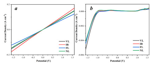
To reveal the photocatalytic mechanism, the interface contacts of steel/TiO2 and TiO2/solution are analyzed. Our previous study demonstrates the ohmic contact between Al and TiO2[16]. As shown in Fig. 13, the I-V characteristics of Al/TiO2/steel also show an ohmic contact between steel and TiO2 due to the lower Fermi energy level (EF) of TiO2 compared to the work function of steel. The band bending effect would accumulate electron in the steel and block the hole migration. Thus, the hydrogen should generate at the surface of steel. A movie clip filmed during photocatalytic experiment clearly shows the generation of hydrogen bubble at the edge of steel rather than on the TiO2 film. As to the interface between TiO2 and aqueous solution, a liquid junction is formed between TiO2 and the solution redox couple (the potential of the formaldehyde oxidation reaction)[25, 26]. Equilibrium could be achieved through the transfer of electrons from TiO2 to aqueous solution. The energy band bends owing to electron depletion in TiO2. And a Schottky barrier formed in TiO2 is expected. Accordingly, the I-V characteristics of TiO2/solution (Fig. 13) show a rectifying behavior.
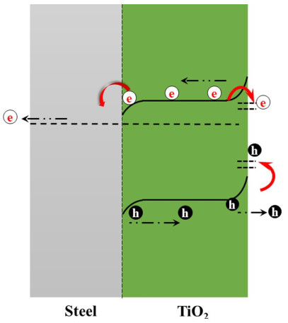
According to the catalytic performance and I-V characteristics, a possible photocatalytic mechanism for hydrogen evolution is presented in Scheme 1. An ohmic contact is formed at the interface of steel and TiO2 film, and Schottky barrier is induced at the interface of TiO2 and solution. Photo-generated electrons are driven by the built-in electric field into steel while the holes are transferred to oxidize the formaldehyde. The enhancement of photocatalytic performance is due to high efficiency in the transferring of photo-generated carriers in the photo-assisted deposited samples. Unlike the nanoparticles with a huge specific surface area, the contact interface between thin film and solution is limited. The defects located on the surface of TiO2 films would significantly hinder the transfer of photo-induced carriers from TiO2 to solution. The ineffective electron transferring would reduce its photocatalytic performance.
TiO2 thin films are deposited on the steel with photo assistance. The columnar grain structure and the nanoparticle morphology show a typical Volmer-Weber growth mode. The films exhibit (101) anatase preferred orientation and a sharp absorption edge. All films demonstrate photocatalytic H2 evolution activity. The Mott-Schottky effect is supposed to promote the separation of photo-generated carrier. Photo-assisted deposited films show an enhanced photocatalytic activity due to the reduction of interface recombination and the high efficiency in the transferring of photo-generated carriers.
Seol, J. S.; Lee, S. Y.; Lee, J. C.; Nam, H. D.; Kim, K. H. Electrical and optical properties of Cu2ZnSnS4 thin films prepared by rf magnetron sputtering process. Sol. Energy Mater. Sol. Cells 2003, 75, 155–162. doi: 10.1016/S0927-0248(02)00127-7
Chang, J. F.; Kuo, H. H.; Leu, I. C.; Hon, M. H. The effects of thickness and operation temperature on ZnO: Al thin film CO gas sensor sens. Actuator B-Chem. 2002, 84, 258–264. doi: 10.1016/S0925-4005(02)00034-5
Carcia, P. F.; McLean, R. S.; Reilly, M. H.; Nunes, G. Transparent ZnO thin-film transistor fabricated by rf magnetron sputtering. Appl. Phys. Lett. 2003, 82, 117–1119.
Ling, B.; Sun, X. W.; Zhao, J. L.; Tan, S. T.; Dong, Z. L.; Yang, Y.; Yu, H. Y.; Qi, K. C. Electroluminescence from a n-ZnO nanorod/p-CuAlO2 heterojunction light-emitting diode. Physica E 2009, 41, 635–639. doi: 10.1016/j.physe.2008.10.017
Fortunato, E. M. C.; Barquinha, P. M. C.; Pimentel, A. C. M. B. G.; Goncalves, A. M. F.; Marques, A. J. S.; Pereira, L. M. N.; Martins, R. F. P. Fully transparent ZnO thin-film transistor produced at room temperature. Adv. Mater. 2005, 17, 90–594.
Okimura, K. Low temperature growth of rutile TiO2 films in modified rf magnetron sputtering. Surf. Coat. Technol. 2001, 135, 86–290.
Yue, L.; Zhou, M. L.; Chen, Q.; Weng, J.; Zhang, Y. F. Ag/PEO nanocomposite fabricated in a planar magnetron sputtering. Vacuum 2009, 83, 1200–1203. doi: 10.1016/j.vacuum.2008.10.006
Yang, I. H.; Lee, Y.; Jang, J. N.; Hong, M. Study of the inductively coupled plasma assisted DC magnetron sputtering (ICPDMS) during ITO deposition. Thin Solid Films 2009, 517, 4165–4169. doi: 10.1016/j.tsf.2009.02.032
Asmussen, J.; Grotjohn, T. A.; Mak, P.; Perrin, M. A. The design and application of electron cyclotron resonance discharges. Ieee T. Plasma Sci. 1997, 25, 1196–1221. doi: 10.1109/27.650896
Ehiasarian, A. P.; Wen, J. G.; Petrov, I. Interface microstructure engineering by high power impulse magnetron sputtering for the enhancement of adhesion. J. Appl. Phys. 2007, 101, 054301. doi: 10.1063/1.2697052
Marinangeli, R. E.; Ollis, D. F. Photo-assisted heterogeneous catalysis with optical fibers II. Nonisothermal single fiber and fiber bundle. AICHE J. 1980, 26, 1000–1008. doi: 10.1002/aic.690260615
Fujita, Y. The reaction mechanisms for precursors in photo-assisted metalorganic-vapor-phase epitaxy growth of ZnSe. J. Cryst. Growth 2000, 221, 382–387. doi: 10.1016/S0022-0248(00)00718-1
Choy, K. L. Chemical vapour deposition of coatings. Prog. Mater. Sci. 2003, 48, 57–170. doi: 10.1016/S0079-6425(01)00009-3
Fujita, S.; Tanabe, A.; Sakamoto, T.; Isemura, M.; Fujita, S. Growth-rate enhancement by senon lamp irradiation in organometallic vapor-phase epitaxy of znse. Jpn. J. Appl. Phys. 1987, 26, L2000–L2002. doi: 10.1143/JJAP.26.L2000
Li, X.; Zhang, B.; Zhu, H.; Dong, X.; Xia, X.; Cui, Y.; Huang, K.; Du, G. Properties of ZnO thin films grown on Si substrates by photo-assisted MOCVD. Appl. Surf. Sci. 2008, 254, 2081–2084. doi: 10.1016/j.apsusc.2007.08.056
Lv, P.; Chen, S.; Huang, F. Controllable phase transformation of titanium dioxide for the high performance polymer solar cells. Sol. Energy Mater. Sol. Cells 2019, 192, 88–93. doi: 10.1016/j.solmat.2018.11.010
Born, M.; Wolf, E.; Hecht, E. Principles of optics: electromagnetic theory of propagation interference and diffraction of light. Phys. Today 2000, 53, 77–78.
Nowak, M. Determination of optical-constants and average thickness of inhomogeneous-rough thin-films using spectral dependence of optical transmittance. Thin Solid Films 1995, 254, 200–210. doi: 10.1016/0040-6090(94)06268-P
Chen, X. B.; Liu, L.; Yu, P. Y.; Mao, S. S. Increasing solar absorption for photocatalysis with black hydrogenated titanium dioxide nanocrystals. Science 2011, 331, 746–750. doi: 10.1126/science.1200448
Naldoni, A.; Allieta, M.; Santangelo, S.; Marelli, M.; Fabbri, F.; Cappelli, S.; Bianchi, C. L.; Psaro, R.; Dal Santo, V. Effect of nature and location of defects on bandgap narrowing in black TiO2 nanoparticles. J. Am. Chem. Soc. 2012, 134, 7600–7603. doi: 10.1021/ja3012676
Wu, Q. P. Ultra-small yellow defective TiO2 nanoparticles for co-catalyst free photocatalytic hydrogen production. Nano Energy 2016, 24, 63–71. doi: 10.1016/j.nanoen.2016.04.004
Katoh, R.; Murai, M.; Furube, A. Transient absorption spectra of nanocrystalline TiO2 films at high excitation density. Chem. Phys. Lett. 2010, 500, 309–312. doi: 10.1016/j.cplett.2010.10.045
Yamakata, A.; Ishibashi, T.; Onishi, H. Time-resolved infrared absorption spectroscopy of photogenerated electrons in platinized TiO2 particles. Chem. Phys. Lett. 2001, 333, 271–277. doi: 10.1016/S0009-2614(00)01374-9
Lee, J.; Li, Z.; Zhu, L. Z.; Xie, S. H.; Cui, X. L. Ti3+ self-doped TiO2 via facile catalytic reduction over Al (acac) 3 with enhanced photoelectrochemical and photocatalytic activities. Appl. Cataly. B-Environ. 2018, 224, 715–724.
Shaner, M. R.; Fountaine, K. T.; Ardo, S.; Coridan, R. H.; Atwater, H. A.; Lewis, N. S. Photoelectrochemistry of core-shell tandem junction n–p+-Si/n-WO3 microwire array photoelectrodes. Energy Environ. Sci. 2014, 7, 779–790.
Gelderman, K.; Lee, L.; Donne, S. W. Flat-band potential of a semiconductor: using the Mott-Schottky equation. J. Chem. Educ. 2007, 84, 685–688.

Figure 8 Photocurrent response of the as-prepared films under zero bias (Ag/AgCl as the reference electrode)

Figure 10 a) Transient absorption spectra of VL and FL after excitation by 300 nm laser pulses, b) Time profiles of transient absorption signals recorded at 500 nm for VL and FL

Figure 13 I-V characteristics of (a) Al/TiO2/steel and (b) steel/TiO2/solution (Ag/AgCl as the reference electrode)
Table 1. Fitted Parameter of Element in the Equivalent Circuit Model of Steel/TiO2/Solution
| Rs (Ω) | Rct (Ω) | CPE (F) | |
| NL | 5.24 | 30.44 | 4.23 × 10⁻⁷ |
| VL | 6.26 | 22.88 | 2.16 × 10⁻⁷ |
| IR | 5.20 | 26.77 | 4.32 × 10⁻⁷ |
| FL | 5.58 | 27.08 | 2.40 × 10⁻⁷ |
 下载: 导出CSV

 扫一扫看文章

扫一扫关注我们


 下载:
下载: