

引用本文:
范黎明, 王时茂, 叶雨琪, 丁博文, 单雪燕, 孟钢, 方晓东. 卤化物钙钛矿微纳阵列的可控制备及应用[J]. 应用化学,
2020, 37(4): 367-379.
doi:
10.11944/j.issn.1000-0518.2020.04.190297

Citation: FAN Liming, WANG Shimao, YE Yuqi, DING Bowen, SHAN Xueyan, MENG Gang, FANG Xiaodong. Recent Advances in Rational Synthesis and Applications of Halide Perovskite Micro/Nano-Arrays[J]. Chinese Journal of Applied Chemistry, 2020, 37(4): 367-379. doi: 10.11944/j.issn.1000-0518.2020.04.190297
Citation: FAN Liming, WANG Shimao, YE Yuqi, DING Bowen, SHAN Xueyan, MENG Gang, FANG Xiaodong. Recent Advances in Rational Synthesis and Applications of Halide Perovskite Micro/Nano-Arrays[J]. Chinese Journal of Applied Chemistry, 2020, 37(4): 367-379. doi: 10.11944/j.issn.1000-0518.2020.04.190297
卤化物钙钛矿微纳阵列的可控制备及应用
摘要:
卤化物钙钛矿不仅具有光吸收系数高、激子束缚能低、载流子迁移率高等优异的光电性能,而且具有缺陷容忍度高、低温溶液法生长、带隙可调等传统半导体不具备的优点,迅速成为光电领域的研究热点之一。在单个光电器件的基础上,开发阵列型器件将推动卤化物钙钛矿在(柔性)光电器件中的应用。但卤化物钙钛矿因对常规有机溶剂较敏感而与现有光刻工艺不兼容,开发适合卤化物钙钛矿的微纳制作工艺尤为重要。本文系统归纳了近年卤化物钙钛矿微纳阵列制备采用的各种策略和方法,分析了不同方法的优缺点和适用性,介绍了卤化物钙钛矿微纳阵列在光电领域的应用,并对该领域目前存在的问题及发展前景进行了展望,以期为新型卤化物钙钛矿光电器件的研究提供参考。
English
Recent Advances in Rational Synthesis and Applications of Halide Perovskite Micro/Nano-Arrays
Abstract:
Owing to fascinating properties including high photon absorption coefficient, low exciton binding energy and high carrier mobility, as well as unique merits including excellent defect tolerance, enabling solution growth at low temperature, and feasibility in band gap tailoring, halide perovskites have attracted significant attention and emerged as one of hot topics in the area of optoelectronics. Exploring perovskite micro/nano-arrays on the basis of existing single micro/nano-wire device would undoubtedly promote their applications in the high-performance integrated (flexible) optoelectronics devices. Unfortunately, poor resistance of halide perovskite to general chemical agents (including water) hinders their integration by traditional photolithography process. Therefore, novel lithographic methodologies are highly required. This review briefly outlines the state-of-the-art progress on the synthesis of halide perovskite micro/nano-arrays, analyzes their merits, and depicts the recent progress of micro/nano-arrays in the area of optoelectronic devices. Finally, the challenges in the current stage and the development prospects in future are discussed to provide useful guidance in exploring novel perovskite based integrated devices in future.
-
Key words:
- halide perovskite
- / micro/nano-arrays
- / optoelectronic devices
- / solution method
-
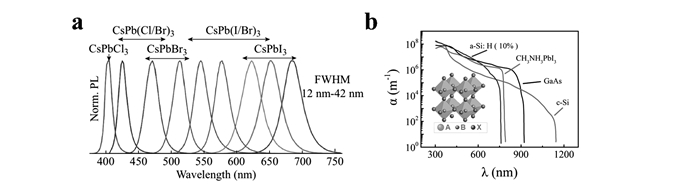
继信息革命之后,以人工智能、虚拟现实、物联网等为代表的智能时代已经到来。光电器件是智能社会中人机交互、数据采集及信息传输等应用的基础之一[1]。以卤化物钙钛矿为代表的新材料的出现为光电器件的进一步发展注入了活力[2-3]。卤化物钙钛矿结构式为ABX3(A位为+1价碱金属或有机阳离子,如Cs+、CH3NH3+、HC(NH2)2+等,B位为+2价金属阳离子,X为卤素离子),与Ⅲ、Ⅵ族半导体类似,卤化物钙钛矿可通过改变X位卤素离子实现带隙的准连续调控[4-6]。图 1(a)展示了CsPbX3(X=Br, Cl, I)的光致发光光谱(PL谱),通过改变阴离子的组分其PL谱可以覆盖407~734 nm波段[7-9];卤化物钙钛矿在紫外-可见波段有较高的光吸收系数,是可以跟Si、GaAs相媲美的高效光吸收介质(图 1(b))[10-12]。卤化物钙钛矿具有独特的缺陷容忍性能,呈现高载流子迁移率、高载流子寿命/扩散距离[13-22]。此外,卤化物钙钛矿还具有传统Si、GaAs等半导体不具备的可低温溶液法生长的独特优势[23-24],有望解决传统Si、GaAs光电器件与柔性衬底不兼容的问题[25-27]。
图 1
自2009年日本科学家Kojima等[17-18]首次使用以来,卤化物钙钛矿已经成为近十年来光电领域的研究热点之一[28-41]。然而,光电器件想要走向实际应用,必须经历阵列化制备的道路。但传统的光刻工艺会对卤化物钙钛矿晶体结构造成破坏,所以需要开发出合适的工艺以制备卤化物钙钛矿微纳阵列[29-31]。同时,阵列化制备的工作可以实现对卤化物钙钛矿微纳晶体进行尺寸上(厚度以及线宽)以及位置上的控制,将促进新器件的研发。因此,在单个光电器件的基础上,开展阵列型单晶器件的开发研究是学术界(有源矩阵显示器、逻辑电路和图像传感器等新型集成器件,包括柔性可穿戴器件)与产业界(器件按标准工艺量产)共同关注的焦点[39-41],有望推动各种光电器件,如电子眼睛、植入式生物医学器件、可穿戴电子器件等的开发研究。
目前卤化物钙钛矿微纳阵列的相关研究已经引起广泛的关注,但是还缺乏具有针对性的、全面的、系统的总结。在这一背景下,本文从溶液法制备卤化物钙钛矿的基本原理出发,梳理了已报道的微纳阵列制备方法,一方面针对不同的情况提供了适合的制备方法,另一方面有望启迪新的制备方法出现。本文还对钙钛矿阵列在各种光电器件中的应用进行了系统的总结,以期对卤化物钙钛矿光电子器件的研究有一定的指导作用。
1. 卤化物钙钛矿微纳阵列制备方法
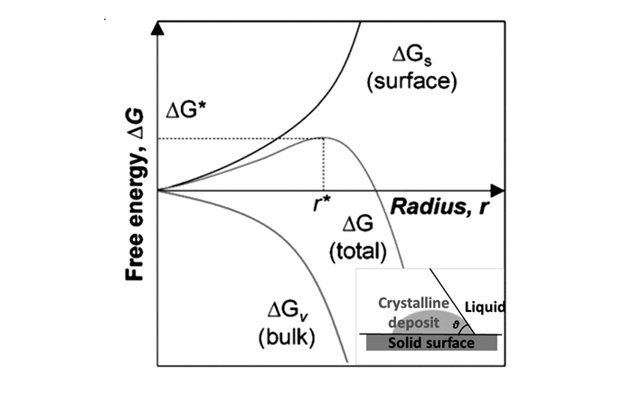
溶液法是制备卤化物钙钛矿微纳阵列使用最多的方法。其主要原理是引导BX2与AX在界面处相互混合、渗透从而生成中间相,然后通过退火获得钙钛矿相[42-49]。卤化物钙钛矿结晶过程以及相转变过程一直伴随着吉布斯自由能的变化(图 2)[49]。随着钙钛矿前驱体溶液溶剂的蒸发,卤化物钙钛矿前驱体溶液达到过饱和的亚稳态[47-49]。在卤化物钙钛矿前驱体溶液与衬底接触的界面,吉布斯自由能相差较大,饱和前驱体溶液优先从亚稳态向钙钛矿相转化[49]。在界面处,当晶核的r>r*时便不断吸收新的粒子凝聚从而增大、生长。由于大部分溶液法制备卤化物钙钛矿微纳阵列的过程属于异相成核,所以不光前驱体溶液配比、结晶速率、结晶温度、气压等参数及条件会影响卤化物钙钛矿晶体成核及生长,前驱体溶液的极性、生长基底的界面能等因素也起着至关重要的作用[50-55]。
图 2
卤化物钙钛矿微纳阵列的制备,重点在于如何简单、高效、高重复率和高精度地实现“图形化”[55-58];然而,常规溶液中形核生长时,形核位置、尺寸和形貌通常随机分布。针对这一问题,Feng等[59]提出了限域生长——将钙钛矿前驱体溶液限域在衬底特定位置(类自上而下)的策略:可通过模板压印的原理实现,即利用有凹凸微纳沟槽的模板将滴在平面衬底上的卤化物钙钛矿前驱体溶液限域在指定区域,经溶剂挥发-晶化后移去模板,获得跟模板互补的微纳阵列[59-62]。另外,鉴于多数卤化物钙钛矿前驱体溶液极性较大,因而可利用自组装单分子(Self-Assembled Monolayer,SAM)修饰的亲水/疏水图形实现前驱体溶液在衬底指定“亲水区”的选择性浸润,限定其在衬底指定区域的结晶,达到图形化生长微纳结构的目的[63]。此外,钙钛矿的图形化也可通过喷墨打印[44]、聚焦激光等直写(类自下而上)[47]等策略获得。
1.1 模板法(template method)
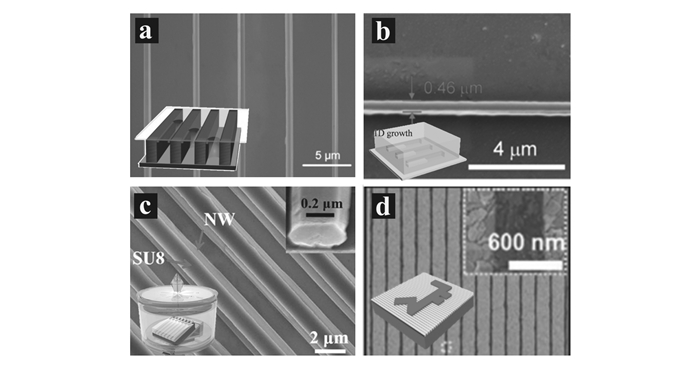
模板法是一种简单、高效的控制钙钛矿前驱体溶液在微纳空间分布/填充的方法[48]。该方法简单、分辨率高,在批量或重复制备卤化物钙钛矿阵列方面具有独特的优势,是一种制备高质量卤化物钙钛矿阵列的重要方法。根据模板模量的不同,模板法可分为图 3中的硬模板法(如SiO2/Si模板)和软模板法(如聚二甲基硅氧烷(Polydimethylsiloxane,PDMS)模板、光刻胶模板、单分子层模板等)。
图 3

1.1.1 SiO2/Si硬模板(SiO2/Si template)
硅基模板杨氏模量高(Si:~150 GPa),可通过湿法、干法(反应离子刻蚀)刻画纳米级别的沟槽,进一步通过表面硅烷化调控表面浸润性后,可实现钙钛矿前驱体溶液的精细限域。在卤化物钙钛矿微纳阵列制备中,最常采用的硬模板为SiO2、Si模板[60]。2017年,Feng等[59]使用SiO2/Si模板得到卤化物钙钛矿微纳单晶阵列(图 3(a))。从图 3(a)插图可以看到,疏水的微槽顶壁与亲水的微槽侧壁拥有很好的空间限域效果,滴入其中的溶液被限制在两个微柱的间隙中,从而形成具有方形截面的毛细管[60]。在溶剂挥发过程中,晶体自身的取向性和毛细管流动起导向作用,在气液固三相接触面上诱导晶体的随机成核和生长。随着钙钛矿前驱体溶液的溶剂蒸发,受毛细拖拽的影响,卤化物钙钛矿单晶会沿SiO2/Si方向高度定向生长,形成卤化物钙钛矿微纳阵列[59]。2019年,Chen等[64]使用SiO2/Si硬模板法制备出了稳定的α-CsPbI3纳米线光电探测器阵列。
SiO2/Si硬模板法限域能力较强、分辨率高(模子不易扭曲变形,线宽最小在400 nm左右)、便于控制尺寸与(特殊)形貌[59-60]等优点。但是由于硬模板杨氏模量较高,只有在超平模板/超平衬底之间才能形成较好的共形接触(conformal contact),若(刚性)衬底平整度不够高、或者使用过程中落入灰尘或颗粒,往往会破坏刚性模板的限域效果。
1.1.2 PDMS模板(PDMS template)
PDMS杨氏模量在MPa量级,是最常用的软模板材料。PDMS模板与硅、玻璃等刚性衬底接触时,即使衬底平整度不高、或者有微小颗粒,PDMS模子均能通过适度变形同衬底形成共形接触,提升限域的效果及成功率[65]。图 3(b)给出了PDMS软模板法的示意图:首先,将制备好的PDMS软模板压到Si片衬底上,然后把卤化物钙钛矿前驱体溶液注入到PDMS软模板与Si片形成的空隙中,溶液在模板的限制下只能分布于模板的凹槽区域,随着溶剂的挥发,卤化物钙钛矿在凹槽区域缓慢结晶。
2017年,Liu等[61-62]利用PDMS软模板约束效应限制MAPbX3前驱体溶液顺着PDMS软模板矩形凹槽的方向分布,成功生长出了卤化物钙钛矿纳米线阵列(图 3(b))。2019年,Gao等[66]使用更灵活的光刻胶软模板制备了卤化物钙钛矿微纳阵列,原理与PDMS软模板类似。总之:软模板制备过程虽然复杂,但使用简单、模板可以重复利用且易于形成共形接触,是一种简单高效的卤化物钙钛矿阵列构筑方法。
1.1.3 光刻胶模板(photoresist template)
2017年,Deng等[40]报道了一种简便的流体导向的反溶剂蒸发辅助结晶方法,制备了图 3(c)中的卤化物钙钛矿微纳阵列。衬底经过光刻处理后表面形成条纹状的光刻胶图案。将带有光刻胶条纹的Si片浸入钙钛矿前驱体的N, N-二甲基甲酰胺(DMF)溶液中。然后,在室温下将模板倾斜放置在含有CH2Cl2反溶剂的称重瓶中密封放置。沿光刻胶带方向生长的卤化物钙钛矿纳米线最窄处线宽达到370 nm。在这个过程中,光刻胶条带不仅为卤化物钙钛矿阵列的生长提供成核位点,而且引导前驱体溶液的定向流体运动,保证了合成纳米线的有序取向。
光刻胶模板法是一种一次性软模板,模板可借用光刻工艺高精、批量获得,模板制备相对于PDMS软模板简便很多,同时所得钙钛矿微纳阵列由于结晶过程缓慢、生长环境与水分隔绝,表面缺陷很少[40]。但由于其在接近光刻胶的地方界面能差异较大、更易结晶从而导致卤化物钙钛矿晶体厚度分布不均匀,可控性略差。此外,微纳阵列生长后光刻胶模板不易去除,会残留在衬底。适用于对厚度起伏要求不高的“条纹状”的单晶微纳阵列。
1.1.4 单分子层模板(SAM template)
由于大部分卤化物钙钛矿前驱体溶液极性较大,因此可通过对衬底局域的亲水性/疏水改性来调控前驱体溶液在指定亲水区域的浸润(限域)生长。2015年,Wang等[67]使用自组装的十八烷基三氯硅烷单分子层(octadecyl- trichlorosilane,OTS)对SiO2/Si基板进行疏水处理,然后利用光刻胶做掩膜进行氧等离子体刻蚀获得亲水图形阵列,成功制备了微米级别的卤化物钙钛矿阵列。2017年,Lee等[63]运用图案化的亲水/疏水单分子层模板结合旋涂加热的方法,通过控制加热温度与转速制备了钙钛矿纳米线在内的多种微纳结构阵列,线宽可以达到600 nm(图 3(d))。
虽然单分子层模板限域能力较弱,但单分子层模板法克服了硬、软模板接触时的残余层问题,同时也避免了厚光刻胶软模板的影响,利用调控前驱体溶液/衬底的界面能来实现图形化生长,方法简单高效、能设计包括线状在内的复杂图形阵列的图形化生长。
1.2 直写法(direct writing method)
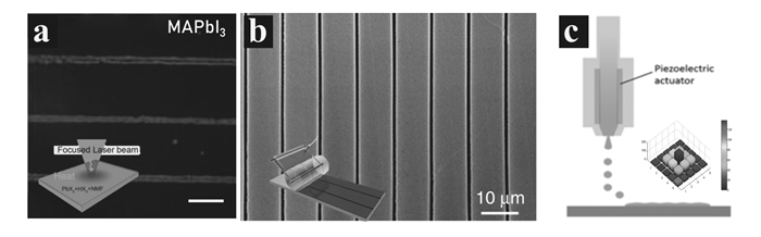
直写法普遍拥有生长过程简单、无需模板和图案灵活等优点,在需要快速、大规模制备卤化物钙钛矿微纳阵列时有一定的优势[47, 68],图 4列举了3种比较有代表性的直写法。
图 4

1.2.1 激光直写(laser direct writing)
2017年,Arciniegas等[47]利用激光的光热效应使用800 nm的激光制备了卤化物钙钛矿微纳阵列(图 4(a))。聚焦激光产生的热量由衬底传递到钙钛矿前驱体液体中,造成局部升温。与此同时,钙钛矿前驱体溶液中的溶剂受热蒸发,慢慢达到过饱和析出结晶。在晶体生长过程中,钙钛矿晶体的分布受温度梯度影响会有所不同。通过调整激光光斑大小、功率密度与辐照时间,调控晶体形状和尺寸[47]。
此方法方便、快捷、无需模板、可灵活设计图形[70-73]。但受限于聚焦激光的光束、及溶剂热扩散的影响,无法获得表面光滑的单晶图形,且线宽比较宽(目前报道的最细线宽是15 μm左右)。
1.2.2 滚轮印刷(ink roller printing)
2017年,Lee等[69]用滚轮印刷的方法得到卤化物钙钛矿阵列,线宽在400 nm左右(图 4(b))。首先将带有图案的柔薄型PDMS包裹在圆柱形不锈钢滚轮上,作为轧制滚轮。将钙钛矿前驱体溶液分布在滚轮的前方并在滚轮滚动的过程中进行加热。在滚轮上面PDMS的几何限制下,滚轮滚过之后卤化物钙钛矿前驱体溶液便会以图案形式分布。然后控制溶剂挥发,经过退火等处理之后得到卤化物钙钛矿微纳阵列。
油墨辊印虽然存在灵活性差、分辨率低等问题,但是其方便快捷、节约成本、可重复利用、可大规模制备。最重要的是,油墨辊印解决了卤化物钙钛矿图形化生长与典型的平版印刷工艺(需利用水油不相混合原理)不兼容(钙钛矿易溶于大部分溶剂)的问题[69, 74]。
1.2.3 油墨喷印(inkjet printing)
2017年,Liu等[44]通过选择合适的溶剂和控制晶体生长速率(图 4(c)),采用喷墨打印的方法不但合成了卤化物钙钛矿微米线、二维网状晶体和岛状晶体,并且进一步制备出卤化物钙钛矿微米线阵列。
油墨喷印制备的卤化物钙钛矿阵列虽然分辨率低(线宽30 μm),但具有方便、快捷、经济等优点,对于制备低成本、高性能的卤化物钙钛矿阵列提供了一种新思路[44, 79]。
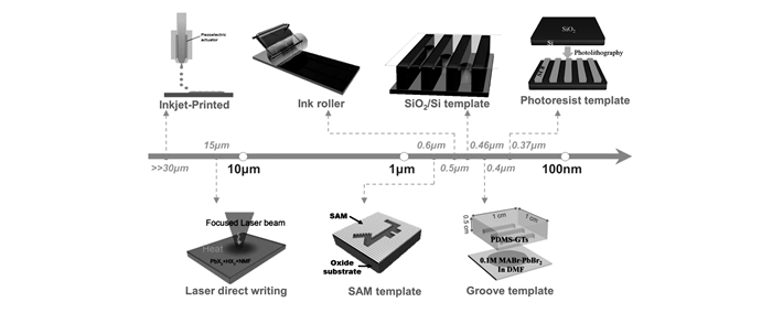
1.3 制备方法汇总与对比
表 1对比了几种图形化方法比较有代表性的工作,而每种方法的极限线宽对比可以从图 5看到。综合表 1与图 5的数据可以看出:模板法提供了一种简易、高效、精细(线宽最小可以达到370 nm[60])的图形化策略,适用于(产业)量产。但在图形设计的灵活性、前后工艺的套刻对准、非平表面刻画等方面存在不足,不能完全满足卤化物钙钛矿器件开发的需求。
表 1

 下载:
导出CSV
下载:
导出CSV
Method Advantages Disadvantages SiO2/Si template high-resolution, reusable complicated PDMS template high-resolution, reusable complicated Photoresist template simple non-reusable, low resolution SAM template high-resolution non-reusable Laser direct writing simple, reusable, controllable low resolution Ink roller high-resolution, reusable, monocrystalline complicated Inkjet printing Simple, reusable low resolution 图 5

相对来说直写的图形化策略图形设计灵活、柔性(甚至非平)衬底兼容、油墨喷印及辊印也满足低成本、高效量产的需求。然而,由于受聚焦光斑尺寸(激光直写)、喷墨打印机分辨率(油墨喷印)、滚轮尺寸(滚轮印刷)等因素的制约,现有直写的分辨率还比较低,大部分线宽都高于10 μm[75-76]。除了文中详细列出的几种方法之外,还可以使用纳米压印[72-76]、毛细直写[68]和电泳法[82-83]等方法制备卤化物钙钛矿阵列。另外,除了溶液法还可以使用气相法[79]制备卤化物钙钛矿阵列[84-86]。气相法的优点是晶体缺陷较少,但普遍存在需要高温、可控性差等缺点[85-87]。
显然,以上每种方法均各有利弊、均有各自适用的场景。同时,每种方法之间也存在相互借鉴的可能,比如2018年Duan等[83]的工作便把硬模板法与旋涂法结合起来使用。所以在开拓新的生长方法的同时,也可以打开思路发展改进已有的生长方法。无疑,今后仍需更深入的研究来推动卤化物钙钛矿微纳阵列制备方法的改进与创新,在提高分辨率的同时降低成本、增强实用性。
2. 卤化物钙钛矿微纳阵列的应用
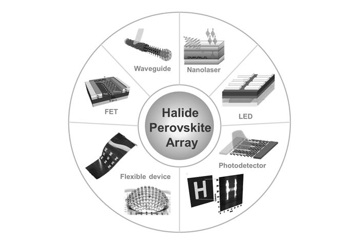
卤化物钙钛矿阵列在光电探测器[11]、场效应晶体管[52]、光波导[53]和激光器[50]等光电器件中均有出色的应用前景(图 6)[46, 89-91]。
图 6

2.1 光电探测器(photodetector)
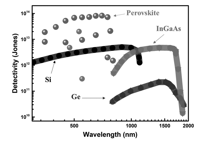
卤化物钙钛矿光吸收系数高、载流子迁移率高、激子束缚能低[87],是优异的光电探测材料。自2014年溶液法生长的卤化物钙钛矿首次用于光电探测器[11]以来,卤化物钙钛矿光电探测器发展迅速[33],2015年便出现了阵列化的卤化物钙钛矿光电转换器件[39]。但直到2017年阵列化的卤化物钙钛矿单晶才开始用于光电探测[40]。图 7对比了卤化物钙钛矿与传统半导体材料(Si、InGaAs、Ge等)在可见光波段的探测率(detectivity)[10, 44, 93-95],可见在大部分报道中卤化物钙钛矿的探测率已经超过传统半导体材料。Feng等[93]使用卤化物钙钛矿单晶纳米线阵列制备的光电探测器,对于530 nm的光源探测率超过了5×10¹⁵ Jones、响应率(responsivity)达到了1.5×10⁴ A/W,已超过现有硅光电探测器。此外,卤化物钙钛矿微纳阵列的低温溶液生长特性也为柔性可穿戴光电探测器的开发奠定了基础[46]。在溶液法制备卤化物钙钛矿阵列的基础上仿动物眼睛制备半球形光电传感器阵列具有广角视野、低像差、高运动灵敏度和无限景深等优点[96-98],为卤化物钙钛矿阵列的应用发展提供了一个研究方向。
图 7

2.2 场效应晶体管(field effect transistor,FET)
2015年,Li等[89]首次报道了MAPbI3薄膜型FET器件,其电子与空穴迁移率分别为0.93与0.31 cm2/(V·s)。同年,Wang等[67]在SiO2/Si衬底上,将MAPbI3单晶微米片作为场效应晶体管的半导体通道,两个金电极作为源极和漏极(通道长度为40 μm),首次制备出了单晶卤化物钙钛矿FET的阵列,电子迁移率可达2.5 cm2(V·s)。
对于FET而言,载流子在横向和界面的传输特别容易受到多晶晶面和晶粒缺陷的影响,2018年,Yu等[99]使用空间限域的方法,采用逆温度生长策略制备了高质量卤化物钙钛矿单晶FET在性能方面得到显著提升。但是,目前还需要研究工作不断深入,以制备高质量的卤化物钙钛矿FET阵列。
2.3 光波导(optical waveguide)
半导体纳米线具有纳米级的直径和微米级别的长度具有较高的折射率,可以同时作为有源增益材料和光波导腔[100],在集成光子领域具有很大的潜力[101]。研究表明,低维卤化物钙钛矿有望减少传波损耗与耦合损耗从而降低功耗提高集成光波导器件的性能。
2015年,Suarez等[53]利用卤化物钙钛矿的发射特性,实现了一种稳定、低功耗的光波导放大器。其增益约为10 db/cm、谱线宽度从50 nm变为3~4 nm、泵浦放大自发辐射(Amplification of Spontaneous Emission,ASE)的能量阈值低至2 nJ,另外通过聚甲基丙烯酸甲酯(Polymethyl Methacrylate,PMMA)封装后,一年之内性能无明显下降。2016年,Wang等使用多晶卤化物钙钛矿微米线制备的光波导器件具有较小的传播损耗。并且可以使用不同卤素的卤化物钙钛矿微米线来传导不同波长的光[102],初步展现了准一维结构的卤化物钙钛矿在微纳光子器件领域的应用潜力。
2.4 激光器(laser)
小型固体激光器的尺寸与衍射极限处于同一个量级,在高密度数据存储、光学集成和高分辨率成像等方向有很好的应用前景[65, 103]。钙钛矿较高的吸收系数和较低的缺陷密度有利于提高激光器的增益[104]。另外,钙钛矿的载流子传输距离较长在微米以及纳米级激光器领域拥有很大的潜力[105]。纳米级的钙钛矿阵列有利于集成的小型激光阵列器件,对于实现大面积、规模化生产大功率激光源有重要作用[106]。
2014年,Deschler等[50]使用卤化物钙钛矿CH3NH3PbI3组成光泵浦垂直腔,制备了图 6的卤化物钙钛矿激光器,具有较低阈值(<200 μJ/cm2)和较窄的谱线宽度(Dk<0.5 nm)。Dhanker等[107]报告的卤化物钙钛矿激光器光致发光(PL)量子效率高达70%,并且光激发后可在1 ps内形成自由载流子,这些自由载流子在10 s到100 s的时间尺度上进行双分子重组。除了钙钛矿微腔外,在2016年Wang等[108-110]还成功地结合了钙钛矿纳米线阵列与硅栅板实现了周期性的纳米激光器阵列。2019年,Zhizhchenko等[80]通过压印的方法制备了厚度为760 nm、直径为小于10 μm的卤化物钙钛矿微盘,使得制造厘米尺寸的微激光器阵列成为可能。
2.5 其它应用
存储器件:金属卤化物钙钛矿因其高开关比、低工作电压和易于制造等优点,被广泛应用于存储器件中,并被认为是氧化物或硫族化合物的替代物[111-113]。2019年,Zou等[112]制备出了一个具有16×16存储单元的存储器阵列,表明了卤化物钙钛矿在高密度、大面积存储设备方面的很大潜力。
射线探测器:卤化物钙钛矿因其良好的电荷输运特性和对光子的高吸收特性,成为射线探测器的热点。2018年,Wang等[87]制备的MAPbBr3单晶阵列用于X射线成像,可以分离出高能量和低能量的X射线信号,同时获得组织和血管的X射线图像。
3. 总结与展望
当下,已经有多种方法可以实现钙钛矿微纳阵列的图形化生长,但在以下3个方面还存在一定的发展空间。1)工艺优化:首先,相比于自由生长纳米线(线宽低至50 nm左右),生长的卤化物钙钛矿微纳阵列的分辨率(目前线宽最窄370 nm左右)还有很大的提升空间;其次,现有的方法都有各自的使用场景,但通用性不强,所以可在现有方法的基础上进行改进或创新,以期发展出同时具有高分辨率、工艺简单、可重复利用等优点的制备方法;最后,集成度更高、结构更加复杂的光电器件的图形化的研究工作还有很大潜力。2)材料方面:双钙钛矿结构、掺杂、原子位替代等方法都将赋予钙钛矿更加广阔的调节空间,通过调节载流子浓度、能级结构等参数有望产生更加高效、便捷的光电器件。3)单晶的卤化物钙钛矿阵列器件:现有的制备方法,大部分只能制备出多晶薄膜。多晶薄膜由于存在大量晶界及表面缺陷,一方面载流子迁移率较低、寿命较短[11],另一方面,化学与热稳定性差、易受湿度与温度等因素的影响分解为BX2与AX[114],因此器件性能不高;相对于多晶薄膜,卤化物钙钛矿单晶(微/纳米线)具有平整的裸露晶面和单晶载流子传输通道,缺陷密度更少、载流子复合几率更低、光生载流子寿命较长[115-118]。现有的微纳米线阵列制备方法具有一定的局限性,改善制备工艺,快速、高效、廉价地制备卤化物钙钛矿微纳单晶阵列是今后工作的重点。
在保证微纳结构形貌、缺陷控制以及图形化精度的同时,依然需要探索新的方法使光电器件拥有更高的光电性能、更加稳定、更加环境友好。另外,制备工艺的简化、成本的降低也会为卤化物钙钛矿光电器件的发展起到一定的促进作用。通过对比总结以往的方法,未来的微纳阵列制备工作可以围绕着以下3个方面开展:晶体生长过程的精细调控、如何提高分辨率、如何器件化。随着基于卤化物钙钛矿的新型(柔性、可穿戴)光电器件的研究继续深入,必将为智能时代的全面到来提供更加坚实的硬件支持。
-
-
[1]
Xue J, Zhu Z, Xu X. Narrowband Perovskite Photodetector-Based Image Array for Potential Application in Artificial Vision[J]. Nano Lett, 2018, 18(12): 7628-7634.
-
[2]
Horvath E, Spina M, Szekrenyes Z. Nanowires of Methylammonium Lead Iodide (CH3NH3PbI3) Prepared by Low Temperature Solution-Mediated Crystallization[J]. Nano Lett, 2014, 14(12): 6761-6766.
-
[3]
Stoumpos C C, Malliakas C D, Kanatzidis M G. Semiconducting Tin and Lead Iodide Perovskites with Organic Cations:Phase Transitions, High Mobilities, and Near-Infrared Photoluminescent Properties[J]. Inorg Chem, 2013, 52(15): 9019-9038.
-
[4]
Zhang F, Zhong H, Chen C. Brightly Luminescent and Color-Tunable Colloidal CH3NH3PbX3(X=Br, I, Cl) Quantum Dots:Potential Alternatives for Display Technology[J]. ACS Nano, 2015, 9(4): 4533-4542.
-
[5]
Fan J, Ma Y, Zhang C. Thermodynamically Self-healing 1D-3D Hybrid Perovskite Solar Cells[J]. Adv Energy Mater, 2018, 8(16): 1703421.
-
[6]
Gao H, Feng J, Pi Y. Bandgap Engineering of Single-Crystalline Perovskite Arrays for High-Performance Photodetectors[J]. Adv Funct Mater, 2018, 28(46): 1804349.
-
[7]
Zhang J, Yang X, Deng H. Low-Dimensional Halide Perovskites and Their Advanced Optoelectronic Applications[J]. Nano-Micro Lett, 2017, 9(3): 36.
-
[8]
Leyden M R, Jiang Y, Qi Y. Chemical Vapor Deposition Grown Formamidinium Perovskite Solar Modules with High Steady State Power and Thermal Stability[J]. J Mater Chem A, 2016, 4(34): 13125-13132.
-
[9]
Saliba M, Correa-Baena J P, Gratzel M. Perovskite Solar Cells:From the Atomic Level to Film Quality and Device Performance[J]. Angew Chem Int Ed Engl, 2018, 57(10): 2554-2569.
-
[10]
Dou L, Yang Y, You J. Solution-Processed Hybrid Perovskite Photodetectors with High Detectivity[J]. Nat Commun, 2014, 5: 5404-5410.
-
[11]
Xia H R, Li J, Sun W T. Organohalide Lead Perovskite Based Photodetectors with Much Enhanced Performance[J]. Chem Commun, 2014, 50(89): 13695-13697.
-
[12]
Lin Q, Armin A, Lyons D M. Low Noise, IR-Blind Organohalide Perovskite Photodiodes for Visible Light Detection and Imaging[J]. Adv Mater, 2015, 27(12): 2060-2064.
-
[13]
Zhu P, Gu S, Shen X. Direct Conversion of Perovskite Thin Films into Nanowires with Kinetic Control for Flexible Optoelectronic Devices[J]. Nano Lett, 2016, 16(2): 871-876.
-
[14]
Chen Y, He M, Peng J. Structure and Growth Control of Organic-Inorganic Halide Perovskites for Optoelectronics:From Polycrystalline Films to Single Crystals[J]. Adv Sci(Weinh), 2016, 3(4): 1500392.
-
[15]
Deng W, Zhang X, Huang L. Aligned Single-Crystalline Perovskite Microwire Arrays for High-Performance Flexible Image Sensors with Long-Term Stability[J]. Adv Mater, 2016, 28(11): 2201-2208.
-
[16]
Xie Z, Liu S F, Qin L X. Refractive Index and Extinction Coefficient of CH3NH3PbI3 Studied by Spectroscopic Ellipsometry[J]. Opt Mater Express, 2014, 5(1): 223789.
-
[17]
Kojima A, Teshima K, Shirai Y. Organometal Halide Perovskites as Visible-Light Sensitizers for Photovoltaic Cells[J]. J Am Chem Soc, 2009, 131(17): 6050-6051.
-
[18]
Jeon N J, Na H, Jung E H. A Fluorene-Terminated Hole-Transporting Material for Highly Efficient and Stable Perovskite Solar Cells[J]. Nat Energy, 2018, 3(8): 682-689.
-
[19]
Im J H, Luo J, Franckevicius M. Nanowire Perovskite Solar Cell[J]. Nano Lett, 2015, 15(3): 2120-2126.
-
[20]
Cao F R, Tian W, Meng L X. Ultrahigh-Performance Flexible and Self-powered Photodetectors with Ferroelectric P(VDF-TrFE)/Perovskite Bulk Heterojunction[J]. Adv Funct Mater, 2019, 29(15): 1808415.
-
[21]
Wong A B, Lai M, Eaton S W. Growth and Anion Exchange Conversion of CH3NH3PbX3 Nanorod Arrays for Light-Emitting Diodes[J]. Nano Lett, 2015, 15(8): 5519-5524.
-
[22]
Fu Y, Zhu H, Schrader A W. Nanowire Lasers of Formamidinium Lead Halide Perovskites and Their Stabilized Alloys with Improved Stability[J]. Nano Lett, 2016, 16(2): 1000-1008.
-
[23]
Gu L, Tavakoli M M, Zhang D. 3D Arrays of 1024-Pixel Image Sensors based on Lead Halide Perovskite Nanowires[J]. Adv Mater, 2016, 28(44): 9713-9721.
-
[24]
Waleed A, Tavakoli M M, Gu L. Lead-free Perovskite Nanowire Array Photodetectors with Drastically Improved Stability in Nanoengineering Templates[J]. Nano Lett, 2016, 17(1): 523-530.
-
[25]
Zhu C, Tang Y, Chen F. Fabrication of Self-Assembly Polycrystalline Perovskite Microwires and Photodetectors[J]. J Cryst Growth, 2016, 454: 121-127.
-
[26]
Spina M, Grimaldi C, Náfrádi B. Rapid Thickness Reading of CH3NH3PbI3 Nanowire Thin Films from Color Maps[J]. Phys Status Solid A, 2016, 213(8): 2017-2023.
-
[27]
Fakharuddin A, Di Giacomo F, Ahmed I. Role of Morphology and Crystallinity of Nanorod and Planar Electron Transport Layers on the Performance and Long Term Durability of Perovskite Solar Cells[J]. J Power Sources, 2015, 283: 61-67.
-
[28]
Li X, Dar M I, Yi C Y. Improved Performance and Stability of Perovskite Solar Cells by Crystal Crosslinking with Alkylphosphonic Acid Omega-Ammonium Chlorides[J]. Nat Chem, 2015, 7(9): 703-711.
-
[29]
Liao Q, Hu K, Zhang H H. Perovskite Microdisk Microlasers Self-assembled from Solution[J]. Adv Mater, 2015, 27(22): 3405-3410.
-
[30]
Yan C, Wang J, Wang X. An Intrinsically Stretchable Nanowire Photodetector with a Fully Embedded Structure[J]. Adv Mater, 2014, 26(6): 943-950.
-
[31]
Song Y M, Xie Y, Malyarchuk V. Digital Cameras with Designs Inspired by the Arthropod Eye[J]. Nature, 2013, 497(7447): 95-99.
-
[32]
He D, Zhang Y, Wu Q. Two-Dimensional Quasi-freestanding Molecular Crystals for High-Performance Organic Field-Effect Transistors[J]. Nat Commun, 2014, 5: 5162-5169.
-
[33]
Spina M, Lehmann M, N fr di B. Microengineered CH3NH3PbI3Nanowire/Graphene Phototransistor for Low-Intensity Light Detection at Room Temperature[J]. Small, 2015, 11(37): 4824-4828.
-
[34]
Shan X, Wang S, Dong W. Flash Surface Treatment of CH3NH3PbI3 Films Using 248 nm KrF Excimer Laser Enhances the Performance of Perovskite Solar Cells[J]. Sol RRL, 2019, 3(7): 1900020.
-
[35]
Wang S, Dong W, Fang X. Credible Evidence for the Passivation Effect of Remnant PbI2 in CH3NHCH3PbICH3 Films in Improving the Performance of Perovskite Solar Cells[J]. Nanoscale, 2016, 8(12): 6600-6608.
-
[36]
Xia R, Yin G, Wang S. Precision Excimer Laser Annealed Ga-Doped ZnO Electron Transport Layers for Perovskite Solar Cells[J]. RSC Adv, 2018, 8(32): 17694-17701.
-
[37]
单雪燕, 王时茂, 孟钢. 钙钛矿太阳电池电子传输层与光吸收层的界面工程[J]. 化学进展, 2019,31,(5): 714-722. SHAN Xueyan, WANG Shimao, MENG Gang. Interface Engineering of Electron Transport Layer/Light Absorption Layer of Perovskite Solar Cells[J]. Prog Chem, 2019, 31(5): 714-722.
-
[38]
丁博文, 王时茂, 陈喆. 无机钙钛矿CsPbX3晶体的低温溶液生长及应用研究进展[J]. 半导体光电, 2019,40,(2): 151-156. DING Bowen, WANG Shimao, CHEN Zhe. Research Progresses in Low Temperature Slution-Growth and Application of Inorganic Perovskite CsPbX3 Crystals[J]. , 2019, 40(2): 151-156.
-
[39]
Deng H, Yang X, Dong D. Flexible and Semitransparent Organolead Triiodide Perovskite Network Photodetector Arrays with High Stability[J]. Nano Lett, 2015, 15(12): 7963-7969.
-
[40]
Deng W, Huang L, Xu X. Ultrahigh-Responsivity Photodetectors from Perovskite Nanowire Arrays for Sequentially Tunable Spectral Measurement[J]. Nano Lett, 2017, 17(4): 2482-2489.
-
[41]
Cheng Z, Lin J. Layered Organic Inorganic Hybrid Perovskites:Structure, Optical Properties, Film Preparation, Patterning and Templating Engineering[J]. CrystEngComm, 2010, 12(10): 2646-2662.
-
[42]
Fu Y, Meng F, Rowley M B. Solution Growth of Single Crystal Methylammonium Lead Halide Perovskite Nanostructures for Optoelectronic and Photovoltaic Applications[J]. J Am Chem Soc, 2015, 137(17): 5810-5818.
-
[43]
Luan M, Song J, Wei X. Controllable Growth of Bulk Cubic-Phase CH3NH3PbI3 Single Crystal with Exciting Room-Temperature Stability[J]. CrystEngComm, 2016, 18(28): 5257-5261.
-
[44]
Liu Y, Li F, Perumal Veeramalai C. Inkjet-Printed Photodetector Arrays Based on Hybrid Perovskite CH3NH3PbI3 Microwires[J]. ACS Appl Mater Interfaces, 2017, 9(13): 11662-11668.
-
[45]
Zhang X, Liu C, Ren G. High-Switching-Ratio Photodetectors Based on Perovskite CH3NH3PbI3 Nanowires[J]. Nanomaterials(Basel), 2018, 8(5): 318-328.
-
[46]
Xia H, Tong S, Zhang C. Flexible and Air-Stable Perovskite Network Photodetectors Based on CH3NH3PbI3/C8BTBT Bulk Heterojunction[J]. Appl Phys Lett, 2018, 112(23): 233301.
-
[47]
Arciniegas M P, Castelli A, Piazza S. Laser-Induced Localized Growth of Methylammonium Lead Halide Perovskite Nano- and Microcrystals on Substrates[J]. Adv Funct Mater, 2017, 27(34): 1701613.
-
[48]
Kawai S, Ishiguro I. Recording Characteristics of Anodic Oxide Films on Aluminum Containing Electrodeposited Ferromagnetic Metals and Alloys[J]. J Electrochem Soc, 1976, 123(7): 1047-1051.
-
[49]
Jung M, Ji S G, Kim G. Perovskite Precursor Solution Chemistry:From Fundamentals to Photovoltaic Applications[J]. Chem Soc Rev, 2019, 48(7): 2011-2038.
-
[50]
Deschler F, Price M, Pathak S. High Photoluminescence Efficiency and Optically Pumped Lasing in Solution-Processed Mixed Halide Perovskite Semiconductors[J]. J Phys Chem Lett, 2014, 5(8): 1421-1426.
-
[51]
Tan Z K, Moghaddam R S, Lai M L. Bright Light-Emitting Diodes Based on Organometal Halide Perovskite[J]. Nat Nanotechnol, 2014, 9(9): 687-692.
-
[52]
Chin X Y, Cortecchia D, Yin J. Lead Iodide Perovskite Light-Emitting Field-Effect Transistor[J]. Nat Commun, 2015, 6: 7383-7392.
-
[53]
Suarez I, Juarez-Perez E J, Bisquert J. Polymer/Perovskite Amplifying Waveguides for Active Hybrid Silicon Photonics[J]. Adv Mater, 2015, 27(40): 6157-6162.
-
[54]
Zhao P, Bian L, Wang L. Enhanced Open Voltage of BiFeO3 Polycrystalline Film by Surface Modification of Organolead Halide Perovskite[J]. Appl Phys Lett, 2014, 105(1): 13901-13906.
-
[55]
Deng H, Dong D, Qiao K. Growth, Patterning and Alignment of Organolead Iodide Perovskite Nanowires for Optoelectronic Devices[J]. Nanoscale, 2015, 7(9): 4163-4170.
-
[56]
Zhuo S, Zhang J, Shi Y. Self-Template-Directed Synthesis of Porous Perovskite Nanowires at Room Temperature for High-Performance Visible-Light Photodetectors[J]. Angew Chem Int Ed, 2015, 54(19): 5693-5696.
-
[57]
Zhu F, Men L, Guo Y. Shape Evolution and Single Particle Luminescence of Organometal Halide Perovskite Nanocrystals[J]. ACS Nano, 2015, 9(3): 2948-2959.
-
[58]
Deng W, Zhang X, Huang L. Aligned Single-Crystalline Perovskite Microwire Arrays for High-Performance Flexible Image Sensors with Long-Term Stability[J]. Adv Mater, 2016, 28(11): 2201-2208.
-
[59]
Feng J, Yan X, Liu Y. Crystallographically Aligned Perovskite Structures for High-Performance Polarization-Sensitive Photodetectors[J]. Adv Mater, 2017, 29(16): 1605993.
-
[60]
Liu Y, Feng J, Zhang B. Regular Aligned 1D Single-Crystalline Supramolecular Arrays for Photodetectors[J]. Small, 2018, 14(5): 1701861.
-
[61]
Liu P, He X, Ren J. Organic-Inorganic Hybrid Perovskite Nanowire Laser Arrays[J]. ACS Nano, 2017, 11(6): 5766-5773.
-
[62]
He X, Liu P, Zhang H. Patterning Multicolored Microdisk Laser Arrays of Cesium Lead Halide Perovskite[J]. Adv Mater, 2017, 29(12): 1604510.
-
[63]
Lee W, Lee J, Yun H. High-Resolution Spin-on-Patterning of Perovskite Thin Films for a Multiplexed Image Sensor Array[J]. Adv Mater, 2017, 29(40): 1702902.
-
[64]
Chen G, Feng J, Gao H. Stable Alpha-CsPbI3 Perovskite Nanowire Arrays with Preferential Crystallographic Orientation for Highly Sensitive Photodetectors[J]. Adv Funct Mater, 2019, 29(13): 1808741.
-
[65]
Yang Z, Lu J F, ZhuGe M H. Controllable Growth of Aligned Monocrystalline CsPbBr3 Microwire Arrays for Piezoelectric-Induced Dynamic Modulation of Single-Mode Lasing[J]. Adv Mater, 2019, 31(18): 1900647.
-
[66]
Gao H, Qiu Y, Feng J. Nano-confined Crystallization of Organic Ultrathin Nanostructure Arrays with Programmable Geometries[J]. Nat Commun, 2019, 10: 3912-3920.
-
[67]
Wang G, Li D, Cheng H C. Wafer-scale Growth of Large Arrays of Perovskite Microplate Crystals for Functional Electronics and Optoelectronics[J]. Sci Adv, 2015, 1(9): 1500613.
-
[68]
Zhao X, Liu T, Shi W. Capillary-Written Single-Crystalline All-Inorganic Perovskite Microribbon Arrays for Highly-Sensitive and Thermal-Stable Photodetectors[J]. Nanoscale, 2019, 11: 2453-2459.
-
[69]
Lee L, Baek J, Park K S. Wafer-scale Single-Crystal Perovskite Patterned Thin Films Based on Geometrically-Confined Lateral Crystal Growth[J]. Nat Commun, 2017, 8: 15882.
-
[70]
Zhizhchenko A, Syubaev S, Berestennikov A. Single-Mode Lasing from Imprinted Halide-Perovskite Microdisks[J]. ACS Nano, 2019, 13(4): 4140-4147.
-
[71]
Spina M, Bonvin E, Sienkiewicz A. Controlled Growth of CH3NH3PbI3 Nanowires in Arrays of Open Nanofluidic Channels[J]. Sci Rep, 2016, 6: 19834.
-
[72]
Chou S S, Swartzentruber B S, Janish M T. Laser Direct Write Synthesis of Lead Halide Perovskites[J]. Chem Lett, 2016, 7: 3736-3741.
-
[73]
Alexander A J. Making Light Work of Crystal Growth A New Method of Stimulating Crystal Growth by Laser Light Could Enhance the Way We Make Materials[J]. Nat Photonics, 2016, 10(11): 694-695.
-
[74]
Mathies F, Eggers H, Richards B S. Inkjet-Printed Triple Cation Perovskite Solar Cells[J]. ACS Appl Energy Mater, 2018, 1(5): 1834-1839.
-
[75]
Bag M, Jiang Z, Renna L A. Rapid Combinatorial Screening of Inkjet-Printed Alkyl-Ammonium Cations in Perovskite Solar Cells[J]. Mater Lett, 2016, 164: 472-475.
-
[76]
Huang J, Lee M, Lucero A. Area-Selective ALD of TiO2 Nanolines with Electron-Beam Lithography[J]. J Phys Chem C, 2014, 118(40): 23306-23312.
-
[77]
Schmager R, Abzieher T, Brenner P, et al. Towards Nano-Patterned Perovskite Layers for Enhanced Absorption In Solar Cells[C]//WCPEC.Hawaii: IEEE, 2018: 0015-0017.
-
[78]
Cefarin N, Cian A, Sonato A. Nanostructuring Methylammonium Lead Iodide Perovskite by Ultrafast Nano Imprinting Lithography[J]. Microelectron Eng, 2017, 176: 106-110.
-
[79]
Wang H, Haroldson R, Balachandran B. Nanoimprinted Perovskite Nanograting Photodetector with Improved Efficiency[J]. ACS Nano, 2016, 10(12): 10921-10928.
-
[80]
Zhizhchenko A, Syubaev S, Berestennikov A. Single-Mode Lasing from Imprinted Halide-Perovskite Microdisks[J]. ACS Nano, 2019, 13(4): 4140-4147.
-
[81]
Cao F R, Tian W, Wang M. Semitransparent, Flexible, and Self-powered Photodetectors Based on Ferroelectricity-Assisted Perovskite Nanowire Arrays[J]. Adv Funct Mater, 2019, 29(24): 1901280.
-
[82]
Rayi V K, Scheidt R A, DuBose J. Hierarchical Arrays of Cesium Lead Halide Perovskite Nanocrystals through Electrophoretic Deposition[J]. J Am Chem Soc, 2018, 140(28): 8887-8894.
-
[83]
Mir W J, Livache C, Goubet N. Strategy to Overcome Recombination Limited Photocurrent Generation in CsPbX3 Nanocrystal Arrays[J]. Appl Phys Lett, 2018, 112(11): 113503.
-
[84]
Lei Y, Gu L Y, Yang X G. Fast Chemical Vapor-Solid Reaction for Synthesizing Organometal Halide Perovskite Array Thin Films for Photodetector Applications[J]. J Alloys Compd, 2018, 766: 933-940.
-
[85]
Wang Y, Yasar M, Luo Z. Temperature Difference Triggering Controlled Growth of All-Inorganic Perovskite Nanowire Arrays in Air[J]. Small, 2018, 14(41): 1803010.
-
[86]
Gao Y, Zhao L, Shang Q. Ultrathin CsPbX3 Nanowire Arrays with Strong Emission Anisotropy[J]. Adv Mater, 2018, 30(31): 1801805.
-
[87]
Wang X, Zhao D W, Qiu Y P. PIN Diodes Array Made of Perovskite Single Crystal for X-Ray Imaging[J]. Phys Status Solidi RRL, 2018, 12(10): 1800380.
-
[88]
Duan Z, Wang Y, Li G. Chip-Scale Fabrication of Uniform Lead Halide Perovskites Microlaser Array and Photodetector Array[J]. Laser Photonics Rev, 2018, 12(1): 1700234.
-
[89]
Li F, Ma C, Wang H. Ambipolar Solution-Processed Hybrid Perovskite Phototransistors[J]. Nat Commun, 2015, 6: 8238.
-
[90]
Zhang Y, Liu J, Wang Z. Synthesis, Properties, and Optical Applications of Low-Dimensional Perovskites[J]. Chem Commun, 2016, 52(94): 13637-13655.
-
[91]
Senanayak S P, Yang B, Thomas T H. Understanding Charge Transport in Lead Iodide Perovskite Thin-Film Field-Effect Transistors[J]. Sci Adv, 2017, 3(1): e1601935.
-
[92]
Chen J, Zhou S, Jin S. Crystal Organometal Halide Perovskites with Promising Optoelectronic Applications[J]. J Mater Chem C, 2016, 4(1): 11-27.
-
[93]
Feng J, Gong C, Gao H. Single-crystalline Layered Metal-Halide Perovskite Nanowires for Ultrasensitive Photodetectors[J]. Nat Electron, 2018, 1(7): 404-410.
-
[94]
Zhou W J, Jin K J, Guo H Z. Electrode Effect on High-Detectivity Ultraviolet Photodetectors Based on Perovskite Oxides[J]. J Appl Phys, 2013, 114(22): 224503.
-
[95]
Gao L, Zeng K, Guo J. Passivated Single-Crystalline CH3NH3PbI3 Nanowire Photodetector with High Detectivity and Polarization Sensitivity[J]. Nano Lett, 2016, 16(12): 7446-7454.
-
[96]
Warrant E, Nilsson D E. Invertebrate vision[M]. Cambridge University Press, 2006.
-
[97]
Dudley R. The Biomechanics of Insect Flight: Form, Function, Evolution[M]. Princeton University Press, 2002.
-
[98]
Kova? M, Zufferey J C, Floreano D. Flying Insects and Robots[M]. Springer, 2009: 271-284.
-
[99]
Yu W, Li F, Yu L. Single Crystal Hybrid Perovskite Field-Effect Transistors[J]. Nat Commun, 2018, 9: 5354-5364.
-
[100]
Zhou H, Yuan S, Wang X. Vapor Growth and Tunable Lasing of Band Gap Engineered Cesium Lead Halide Perovskite Micro/Nanorods with Triangular Cross Section[J]. ACS Nano, 2016, 11(2): 1189-1195.
-
[101]
Piccione B, Cho C H, Van Vugt L K, et al. All-optical Active Switching in Individual Semiconductor Nanowires[J]. Nat Nanotechnol, 2012, 7(10): 640-646.
-
[102]
Wang Z, Liu J, Xu Z Q. Wavelength-tunable Waveguides Based on Polycrystalline Organic-Inorganic Perovskite Microwires[J]. Nanoscale, 2016, 8(12): 6258-6264.
-
[103]
Blanche P A, Bablumian A, Voorakaranam R. Holographic Three-Dimensional Telepresence Using Large-Area Photorefractive Polymer[J]. Nature, 2010, 468(7320): 80-83.
-
[104]
Bar-On O, Brenner P, Lemmer U, et al. Perovskite Micro Laser Arrays Using Scalable Lithography: Towards Integrated Perovskite Photonics[C]//CLEO San Jose: IEEE, 2019.
-
[105]
Xing G, Mathews N, Lim S S. Low-temperature Solution-Processed Wavelength-Tunable Perovskites for lasing[J]. Nat Mater, 2014, 13(5): 476-481.
-
[106]
Zhang Q, Su R, Du W. Advances in Small Perovskite-Based Lasers[J]. Small Methods, 2017, 1(9): 1700163.
-
[107]
Dhanker R, Brigeman A N, Larsen A V. Random Lasing in Organo-Lead Halide Perovskite Microcrystal Networks[J]. Appl Phys Lett, 2014, 105(15): 151112.
-
[108]
Wang K, Gu Z, Liu S. High-Density and Uniform Lead Halide Perovskite Nanolaser Array on Silicon[J]. J Phys Chem Lett, 2016, 7(13): 2549-2555.
-
[109]
Feng J, Yan X, Zhang Y. "Liquid Knife" to Fabricate Patterning Single-Crystalline Perovskite Microplates toward High-Performance Laser Arrays[J]. Adv Mater, 2016, 28(19): 3732-3741.
-
[110]
Wu Z, Chen J, Mi Y. All-Inorganic CsPbBr3 Nanowire Based Plasmonic Lasers[J]. Adv Opt Mater, 2018, 6(22): 1800674.
-
[111]
Kang K, Ahn H, Song Y. High-Performance Solution-Processed Organo-Metal Halide Perovskite Unipolar Resistive Memory Devices in a Cross-Bar Array Structure[J]. Adv Mater, 2019, 31(21): 1804841.
-
[112]
Zou C, He L, Lin L Y. Vacuum-Deposited Inorganic Perovskite Memory Arrays with Long-Term Ambient Stability[J]. Phys Status Solidi RRL, 2019, 13(9): 1900182.
-
[113]
Zou C, Zheng J J, Chang C. Nonvolatile Rewritable Photomemory Arrays Based on Reversible Phase-Change Perovskite for Optical Information Storage[J]. Adv Opt Mater, 2019, 7(18): 1900558.
-
[114]
Li X, Dar M I, Yi C. Improved Performance and Stability of Perovskite Solar Cells by Crystal Crosslinking with Alkylphosphonic Acid Omega-Ammonium Chlorides[J]. Nat Chem, 2015, 7(9): 703-711.
-
[115]
Guo N, Hu W, Liao L. Anomalous and Highly Efficient InAs Nanowire Phototransistors Based on Majority Carrier Transport at Room Temperature[J]. Adv Mater, 2014, 26(48): 8203-8209.
-
[116]
Peng L, Hu L, Fang X. Energy Harvesting for Nanostructured Self-Powered Photodetectors[J]. Adv Funct Mater, 2014, 24(18): 2591-2610.
-
[117]
Liu X, Liu X, Wang J. Transparent, High-Performance Thin-Film Transistors with an InGaZnO/Aligned-SnO2-Nanowire Composite and their Application in Photodetectors[J]. Adv Mater, 2014, 26(43): 7399-7404.
-
[118]
Zhou X, Lu M Y, Lu Y J. Nanoscale Optical Properties of Indium Gallium Nitride/Gallium Nitride Nanodisk-in-Rod Heterostructures[J]. ACS Nano, 2015, 9(3): 2868-2875.
-
[1]
-

表 1 不同方法的综合对比[40, 44, 47, 59-63, 69]
Table 1. Comparison of different methods[40, 44, 47, 59-63, 69]
Method Advantages Disadvantages SiO2/Si template high-resolution, reusable complicated PDMS template high-resolution, reusable complicated Photoresist template simple non-reusable, low resolution SAM template high-resolution non-reusable Laser direct writing simple, reusable, controllable low resolution Ink roller high-resolution, reusable, monocrystalline complicated Inkjet printing Simple, reusable low resolution  下载: 导出CSV
-



 扫一扫看文章
计量
- PDF下载量: 37
- 文章访问数: 2923
- HTML全文浏览量: 731
 下载:
下载:

