Key Laboratory of Beijing City on Preparation and Processing of Novel Polymer Materials, College of Materials Science and Engineering, Beijing University of Chemical Technology, Beijing 100029, China
Corresponding author:
SHI Ling, professor; Tel/Fax:010-64438296; E-mail:shiling@mail.buct.edu.cn; Research interests:functional polymer preparation
Received Date:
14 September 2018 Accepted Date:
17 December 2018 Revised Date:
16 November 2018 Available Online:
10 March 2019
Abstract:
Graphene is a two-dimensional material with excellent properties such as good electrical and thermal conductivity, high carrier mobility, and good transmissivity endowed by its sp2 hybrid planar honeycomb structure. It shows great application prospect in electronic devices. This article reviewed the research progress in the application of graphene in integrated circuits, graphene field effect transistors, graphene organic light-emitting diodes, and chemical sensors.
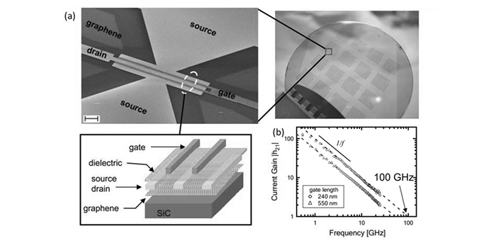
Figure 3.
Scanning electron microscope image and the schematic cross-sectional view of a topgated graphene field-effect transistor(a) and current gain as a function of frequency(b)[24]
Figure 5.
(a)Schematic illustration of TFMS-doped grapheme. (b)Schematic illustration of energy band diagram. (c)Luminance of TFMS-doped 4LG anode on the PET substrate[42]
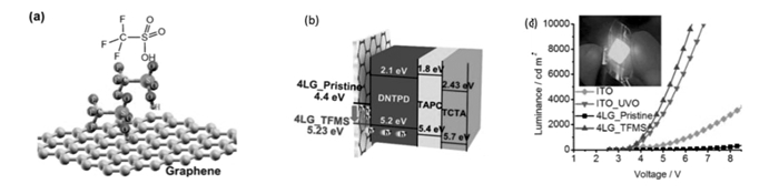
Figure 6.
Schematic illustration of CsF-doped grapheme(a). Sheet resistance and transmittance at 500 nm of pristine and CsF-doped graphene with number of layers(b). Transmittance of three different OLEDs(c). The current density versus voltage(J-V) curves(d)[48]
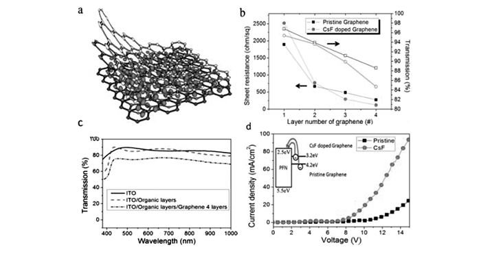
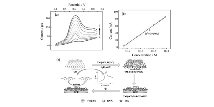
Figure 7.
(a)DPV response at the TM-b-CD-Gr/PtNPs/GCE in 0.1 mol/L phosphate buffer(pH=7.0) for different concentrations of BPA(from a to i):0.050, 0.10, 0.50, 1.0, 5.0, 10, 30, 50 and 80 mmol/L; (b)Calibration graph between the oxidation peak current and the BPA concentration(logarithm). The measurements were repeated three times to obtain the standard deviation; (c)Schematic of the procedure for the synthesis of TM-b-CDGr/PtNPs and the detection of BPA using an electrochemical strategy[53]
Novoselov K S, Geim A K, Morozov S V. Electric Field Effect in Atomically Thin Carbon Films[J]. Science,
2004, 306(5696):
666-669.
doi: 10.1126/science.1102896
[2]
Hummers W S, Offeman R E. Preparation of Graphitic Oxide[J]. J Am Chem Soc,
1958, 80(6):
1339-1339.
doi: 10.1021/ja01539a017
[3]
Reina A, Jia X, Ho J. Large Area, Few-Layer Graphene Films on Arbitrary Substrates by Chemical Vapor Deposition[J]. Nano Lett,
2009, 9(1):
30-35.
doi: 10.1021/nl801827v
[4]
Kageshima H, Hibino H, Nagase M. Theoretical Study of Epitaxial Graphene Growth on SiC(0001) Surfaces[J]. Appl Phys Express,
2009, 2(6):
5502.
[5]
Ping G, Zhang J, Cheng J. Graphene Nanosheets Prepared by Low-Temperature Exfoliation and Reduction Technique Toward Fabrication of High-Performance Poly(1-butene)/graphene Films[J]. Iran Polym J,
2016, 26(1):
1-15.
[6]
Liang K, Shi L, Zhang J. Fabrication of Shape-Stable Composite Phase Change Materials Based on Lauric Acid and Graphene/Graphene Oxide Complex Aerogels for Enhancement of Thermal Energy Storage and Electrical Conduction[J]. Thermochim Acta,
2018, 664:
1-15.
doi: 10.1016/j.tca.2018.04.002
[7]
Lee C, Wei X, Kysar J W. Measurement of the Elastic Properties and Intrinsic Strength of Monolayer Graphene[J]. Science,
2008, 321(5887):
385-388.
doi: 10.1126/science.1157996
[8]
Chen J H, Jang C, Xiao S D. Intrinsic and Extrinsic Performance Limits of Graphene Deviceson SiO2[J]. Nat Nanotechnol,
2008, 3(4):
206-209.
doi: 10.1038/nnano.2008.58
[9]
Balandin A A, Ghosh S, Bao W. Superior Thermal Conductivity of Single-Layer Graphene[J]. Nano Lett,
2008, 8(3):
902-907.
doi: 10.1021/nl0731872
[10]
Nair R R, Blake P, Grigorenko A N. Fine Structure Constant Defines Visual Tranparency of Graphene[J]. Science,
2008, 320(5881):
1308.
doi: 10.1126/science.1156965
[11]
Lin Y M, Valdes-Garcia A, Han S J. Wafer-Scale Graphene Integrated Circuit[J]. Science,
2011, 332(6035):
1294-1297.
doi: 10.1126/science.1204428
[12]
Guo D, Hen S J, Lin C H, et al. Graphene Based Three-Dimensional Integrated Circuit Device: US, US8895372[P]. 2014.
[13]
Pak J S, Pathak M, Lim S K, et al. Modeling of Electromigration in Through-Silicon-Via Based 3D IC[C]//Electronic Components and Technology Conference. IEEE, 2011, 301(4): 1420-1427.
[14]
Chiariello A G, Maffucci A, Miano G. Modeling Carbon Nanotube Bundles for Future On-Chip Nano-interconnects[C]//Electrical Design of Advanced Packaging and Systems Symposium. IEEE, 2011: 1-4.
[15]
Hossain N M, Hossain M, Yousuf A H B, et al. Thermal Aware Graphene Based Through Silicon via Design for 3D IC[C]//3D Systems Integration Conference. IEEE, 2013: 1-4.
[16]
班涛, 潘中良, 陈翎. 使用石墨烯导热层三维集成电路的散热方法研究[J]. 电子技术与软件工程,
2018(5): 99-101.
BAN Tao, PAN Zhongliang, CHEN Ling. Study on Heat Dissipation Method of Three-Dimensional Integrated Circuit Using Graphene Heat Conduction Layer[J]. Electron Technol Software Eng,
2018, (5):
99-101.
[17]
杜.具有石墨烯屏蔽体的三维(3D)集成电路(3DIC)以及相关的制造方法: CN 104981899 A[P]. 2015.Y·DU. Three-Dimensional(3D) Integrated Circuit(3DIC) with Graphene Shield and Related Manufacturing Methods: CN 104981899 A[P]. 2015(in Chinese). Y·
[18]
Han S J, Garcia A V, Oida S. Graphene Radio Frequency Receiver Integrated Circuit[J]. Nat Commun,
2014, 5(1):
3086.
doi: 10.1038/ncomms4086
[19]
Seul K H, Choong S K, Wan S H. Hybrid Integration of Graphene Analog and Silicon Complementary Metal-Oxide-Semiconductor Digital Circuits[J]. ACS Nano,
2016, 10(7):
7142-7146.
doi: 10.1021/acsnano.6b03382
[20]
Ma R, Chen Q, Zhang W. A Dual-Polarity Graphene NEMS Switch ESD Protection Structure[J]. IEEE Electron Device Lett,
2016, 37(5):
674-676.
doi: 10.1109/LED.2016.2544343
王聪, 刘玉荣. 基于石墨烯场效应晶体管的研究进展[J]. 半导体技术,
2016(8): 561-569.
WANG Chong, LIU Yurong. Research Progress on Graphene-Based Field Effect Transistor[J]. Semicond Technol,
2016, (8):
561-569.
[23]
Wang H, Nezich D, Kong J. Graphene Frequency Multipliers[J]. IEEE Electron Device Lett,
2009, 30(5):
547-549.
doi: 10.1109/LED.2009.2016443
[24]
Lin Y M, Dimitrakopoulos C, Jenkins K A. 100-GHz Transistors from Wafer-Scale Epitaxial Graphene[J]. Science,
2010, 327(5966):
662-662.
doi: 10.1126/science.1184289
[25]
Wu Y, Lin Y M, Bol A A. High-Frequency, Scaled Graphene Transistors on Diamond-Like Carbon[J]. Nature,
2011, 472(7341):
74-78.
doi: 10.1038/nature09979
[26]
Cheng R, Bai J, Liao L. High-Frequency Self-aligned Graphene Transistors with Transferred Gate Stacks[J]. Proc Nat Acad Sci USA, Early Ed,
2012, 109(29):
11588-11592.
doi: 10.1073/pnas.1205696109
[27]
Guo Z, Dong R, Chakraborty P S. Record Maximum Oscillation Frequency in C-Face Epitaxial Graphene Transistors[J]. Nano Lett,
2013, 13(3):
942-947.
doi: 10.1021/nl303587r
[28]
Feng Z H, Yu C, Li J. An Ultra Clean Self-aligned Process for High Maximum Oscillation Frequency Graphene Transistors[J]. Carbon,
2014, 75(10):
249-254.
[29]
Wu Y, Zou X, Sun M. 200 GHz Maximum Oscillation Frequency in CVD Graphene Radio Frequency Transistors[J]. ACS Appl Mater Interfaces,
2016, 8(39):
25645-25649.
doi: 10.1021/acsami.6b05791
[30]
Novoselov K S, Geim A K, Morozov S V. Two-Dimensional Gas of Massless Dirac Fermions in Graphene[J]. Nature,
2005, 438(7065):
197-200.
doi: 10.1038/nature04233
[31]
Wessely P J, Wessely F, Birinci E. Silicon-CMOS Compatible In-Situ CCVD Grown Graphene Transistors with Ultra-high On/Off-Current Ratio[J]. Phys E(Amsterdam, Neth),
2012, 44(7/8):
1132-1135.
[32]
Wessely A P J, Schwalke U. 2nd Generation Bilayer Graphene Transistors for Applications in Nanoelectronics[C]//IEEE International Conference on Design & Technology of Integrated Systems in Nanoscale Era. IEEE, 2014: 1-3.
[33]
Si Y L, Duong D L, Vu Q A. Chemically Modulated Band Gap in Bilayer Graphene Memory Transistors with High On/Off Ratio[J]. ACS Nano,
2015, 9(9):
9034-9042.
doi: 10.1021/acsnano.5b03130
[34]
Dragoman M, Dinescu A, Dragoman D. Room Temperature Nanostructured Graphene Transistor with High On/Off Ratio[J]. Nanotechnology,
2016, 28:
015201.
[35]
Dragoman M, Dinescu A, Dragoman D. Solving the Graphene Electronics Conundrum:High Mobility and High On-Off Ratio in Graphene Nanopatterned Transistors[J]. Phys E(Amsterdam, Neth),
2018, 97:
296-301.
doi: 10.1016/j.physe.2017.12.011
Meyer J, Kidambi P R, Bayer B C. Metal Oxide Induced Charge Transfer Doping and Band Alignment of Graphene Electrodes for Efficient Organic Light Emitting Diodes[J]. Sci Rep,
2014, 4:
5380.
[40]
Kwon K C, Choi K S, Kim S Y. Increased Work Function in Few-Layer Graphene Sheets via Metal Chloride Doping[J]. Adv Funct Mater,
2012, 22(22):
4724-4731.
doi: 10.1002/adfm.v22.22
[41]
Kim D, Lee D, Lee Y. Work-Function Engineering of Graphene Anode by Bis(trifluoromethanesulfonyl)amide Doping for Efficient Polymer Light-Emitting Diodes[J]. Adv Funct Mater,
2013, 23(40):
5049-5055.
doi: 10.1002/adfm.v23.40
[42]
Han T H, Kwon S J, Li N. Versatile p-Type Chemical Doping to Achieve Ideal Flexible Graphene Electrodes[J]. Angew Chem Int Ed Engl,
2016, 128(21):
6305-6309.
doi: 10.1002/ange.201600414
[43]
D'Arsiè L, Esconjauregui S, Weatherup R. Stable and Efficient p-Type Doping of Graphene by Nitric Acid[J]. RSC Adv,
2016, 6(114):
113185-113192.
doi: 10.1039/C6RA23727D
[44]
Wu T L, Yeh C H, Hsiao W T. High-Performance Organic Light-Emitting Diode with Substitutionally Boron-Doped Graphene Anode[J]. ACS Appl Mater Interfaces,
2017, 9(17):
14998-15004.
doi: 10.1021/acsami.7b03597
[45]
Cha M J, Song W, Kim Y. Long-Term Air-Stable n-Type Doped Graphene by Multiple Lamination with Polyethyleneimine[J]. RSC Adv,
2014, 4(71):
37849-37853.
doi: 10.1039/C4RA04518A
[46]
Sanders S, Cabrero-Vilatela A, Kidambi P R. Engineering High Charge Transfer n-Doping of Graphene Electrodes and Its Application to Organic Electronics[J]. Nanoscale,
2015, 7(30):
13135-13142.
doi: 10.1039/C5NR03246F
[47]
Zhuo Q Q, Wang Q, Zhang Y P. Transfer-Free Synthesis of Doped and Patterned Graphene Films[J]. ACS Nano,
2015, 9(1):
594-601.
doi: 10.1021/nn505913v
[48]
Chang J H, Lin W H, Wang P C. Solution-Processed Transparent Blue Organic Light-Emitting Diodes with Graphene as the Top Cathode[J]. Sci Rep,
2015, 5:
9693.
doi: 10.1038/srep09693
[49]
Kwon S J, Han T H, Kim Y H. Solution-Processed n-Type Graphene Doping for Cathode in Inverted Polymer Light-Emitting Diodes[J]. ACS Appl Mater Interfaces,
2018, 10(5):
4874-4881.
doi: 10.1021/acsami.7b15307
[50]
Schedin F, Geim A K, Morozov S V. Detection of Individual Gas Molecules Adsorbed on Graphene[J]. Nat Mater,
2006, 6(9):
652-655.
[51]
Fowler J D, Allen M J, Tung V C. Practical Chemical Sensors from Chemically Derived Graphene[J]. ACS Nano,
2009, 3(2):
301-306.
doi: 10.1021/nn800593m
[52]
Wang Z, Zhao C, Han T. High-Performance Reduced Graphene Oxide-Based Room-Temperature NO2, Sensors:A Combined Surface Modification of SnO2, Nanoparticles and Nitrogen Doping Approach[J]. Sens Actuators B,
2017, 242:
269-279.
doi: 10.1016/j.snb.2016.10.101
[53]
Zou J F, Liu Z G, Guo Y J. Electrochemical Sensor for the Facile Detection of Trace Amounts of Bisphenol a Based on Cyclodextrin-Functionalized Graphene/Platinum Nanoparticles[J]. Anal Methods,
2017, 9(1):
134-140.
doi: 10.1039/C6AY02719A
[54]
Sakthinathan S, Kubendhiran S, Chen S. Metallated Porphyrin Noncovalent Interaction with Reduced Graphene Oxide-Modified Electrode for Amperometric Detection of Environmental Pollutant Hydrazine[J]. Appl Organomet Chem,
2017, 31(9):
1-10.
[55]
Seekaew Y, Phokharatkul D, Wisitsoraat A. Highly Sensitive and Selective Room-Temperature NO2, Gas Sensor Based on Bilayer Transferred Chemical Vapor Deposited Graphene[J]. Appl Surf Sci,
2017, 404:
357-363.
doi: 10.1016/j.apsusc.2017.01.286
[56]
Guo L, Kou X, Ding M. Reduced Graphene Oxide/α-Fe2O3, Composite Nanofibers for Application in Gas Sensors[J]. Sens Actuators B,
2017, 244:
233-242.
doi: 10.1016/j.snb.2016.12.137
[57]
Luan F, Zhang S, Chen D. CoS2-Decorated Ionic Liquid-Functionalized Graphene as a Novel Hydrazine Electrochemical Sensor[J]. Talanta,
2018, 182:
529-535.
doi: 10.1016/j.talanta.2018.02.031
[58]
Chu J, Wang X, Wang D. Highly Selective Detection of Sulfur Hexafluoride Decomposition Components H2S and SOF2, Employing Sensors Based on Tin Oxide Modified Reduced Graphene Oxide[J]. Carbon,
2018, 135:
95-103.
doi: 10.1016/j.carbon.2018.04.037
[59]
Rumyantsev S, Liu G, Shur M S. Selective Gas Sensing with a Single Pristine Graphene Transistor[J]. Nano Lett,
2012, 12(5):
2294-2298.
doi: 10.1021/nl3001293
Figure 3
Scanning electron microscope image and the schematic cross-sectional view of a topgated graphene field-effect transistor(a) and current gain as a function of frequency(b)[24]
Figure 5
(a)Schematic illustration of TFMS-doped grapheme. (b)Schematic illustration of energy band diagram. (c)Luminance of TFMS-doped 4LG anode on the PET substrate[42]
Figure 6
Schematic illustration of CsF-doped grapheme(a). Sheet resistance and transmittance at 500 nm of pristine and CsF-doped graphene with number of layers(b). Transmittance of three different OLEDs(c). The current density versus voltage(J-V) curves(d)[48]
Figure 7
(a)DPV response at the TM-b-CD-Gr/PtNPs/GCE in 0.1 mol/L phosphate buffer(pH=7.0) for different concentrations of BPA(from a to i):0.050, 0.10, 0.50, 1.0, 5.0, 10, 30, 50 and 80 mmol/L; (b)Calibration graph between the oxidation peak current and the BPA concentration(logarithm). The measurements were repeated three times to obtain the standard deviation; (c)Schematic of the procedure for the synthesis of TM-b-CDGr/PtNPs and the detection of BPA using an electrochemical strategy[53]

 下载:
下载:


 下载:
下载:


 下载:
下载:
