图 1
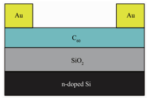
Schematic diagram of the fabricated C60 TFTs
Figure 1.
Schematic diagram of the fabricated C60 TFTs
Effect of Crystallinity and Grain Size of Film on Mobility of C60 Thin Film Transistors
Yi LI , Xiao HAN , Zhi-Peng SUN , Yan-Wen MA

In recent decades, organic thin film transistors (OTFTs) have received considerable attention owing to their low cost, low temperature process, compatibility with plastic substrate, and wide potential applications in large-area, lightweight, flexible electronics devices such as electronic displays, organic memories, and sensors[1-5]. Much research work has been focused on obtaining high performance OTFTs comparable to those of amorphous silicon thin film transistors (TFTs)[6-10]. In addition to the optimization of device structure and performance, the correlation of the charge transport with the thin-film microstructure has also been extensively studied. It is well known that the charge transfer in OTFTs highly rely on the crystallinity, molecular ordering and crystal grain sizes, which in turn depend on the molecular structures of the organic semiconductors[11-12], deposition process[13-16], and substr-ates[17-18]. For the most planar organic semiconducrors molecules, such as CuPc, F16CuPc, pentacene, perylene bisimide and oligothiophene, increasing substrate temperature (Ts), decreasing deposition rate, and incre-asing deposition pressure in vacuum deposition process normally leads to a highly ordered film with larger grain sizes and fewer grain boundaries, which is regarded as the most effective way to obtain high-mobility devices[14-25]. However, for the spherical C60 semiconductor, which is an important n-type semi-conductor material with high mobility, the mechanism of charge transport in C60 films is still unclear, and the relationship between mobility and microstructure of the C60 films is controversial[20, 26-28]. Therefore, it is essential to investigate the effect of morphology and structure, which are quite sensitive to growth condi-tions, on the performance of the C60 films in-depth. In this study, the crystallinity and grain size of the C60 films have been regulated by changing the Ts and deposition pressure in the vacuum deposition process. X-ray diffraction (XRD) and atomic force microscopy (AFM) were used to investigate the morphology and crystalline structure of thin films. Furthermore, the mobilities of the films are obtained by field-effect measurements, and the correlations of mobility with crystallinity and grain size of the C60 films are established.
Fig. 1 shows the schematic diagram of the fabricated C60 TFTs. C60 (99.9%) is purchased from Aldrich and used without further purification. The substrate is 300 nm SiO2 thermally grown on a heavily doped n-Si wafer, which were ultrasonically cleaned with acetone, isopropyl alcohol, and ultrapurified water, successively. A bottom-gate, top-contact device configuration of C60 TFTs was adopted. First, the substrate was set in the chamber and maintained at 4×10⁻⁵ Pa. Subsequently, a 40 nm thick C60 active layer[16], patterned through a shadow mask, was deposited by vacuum evaporation onto the substrate under a specific Ts (i.e., 30, 60, 90, 130, 160 and 190 ℃) at the same rate of 0.01 nm·s-1 recorded by a quartz crystal oscillator. Finally, the gold (Au, 99.99%) electrodes, with a thickness of 50 nm, were defined on the C60 film by thermal evaporation through another mask. For the samples of different deposition pressure, the films were deposited by vacuum deposition under a specific Pdep (i.e. 1×10⁻⁴ and 1×10⁻¹ Pa) with the rate of 0.01 nm·s-1 and the Ts of 130 ℃.The channel length (L) and width (W) are 70 and 500 μm, respectively.
The structures and surface morphologies of the films were characterized by X-ray diffraction (XRD, Philips X′pert Pro X-ray diffractometer in 2θ range of 15°~28°, Cu Kα1 radiation of 0.154 nm) and atomic force microscopy (AFM, Bruker Dimension Icon, tapping Mode). The performances of the devices were evaluated by semiconductor characterization system (Keithley model 4200-SCS) under vacuum condition at room temperature.
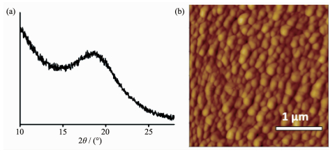
The characteristic XRD patterns and morpho-logies of the C60 films deposited under different Ts are shown in Fig. 2. The XRD patterns of the C60 films show broadened (113) peaks, corresponding to the D values of ca. 1.54 nm. With increasing Ts from 30 to 190 ℃, the intensity of (113) peaks increase, indicating the increased crystallinity of the films (Fig. 2A). The morphological evolutions of the C60 films with Ts are demonstrated in Fig. 2B. It is clearly seen, the grain sizes keep almost unchanged for Ts below 90 ℃(Fig. 2B(a~c)), and gradually increase for further increasing Ts from 90 to 190 ℃ (Fig. 2B(d~f)). The root-mean-square roughness of all the samples obtained from the AFM measurements are about 1~3 nm, indicating the smooth surfaces of the films.
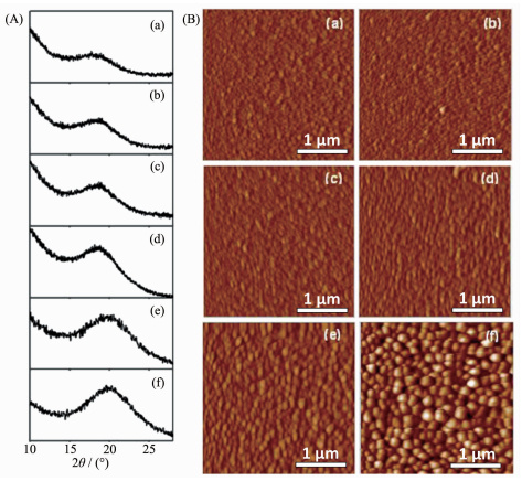
Fig. 3 shows the output characteristics of C60 TFTs prepared under different Ts. The C60 TFTs exhibit typical n-channel field-effect behavior, operated under a positive voltage source-drain voltage (Vd) and gate voltage (Vg), with distinct linear and saturation regions in the output curves. With increasing Ts from 30 to 130 ℃, a significant increase of saturation drain current (Id) from 1.8 to 12.3 μA is observed when they are biased at Vd=60 V and Vg=60 V (Fig. 3a~d). With further increasing Ts to 160 and 190 ℃, Id decreases to 4.2 μA and 2.1 μA, respectively.
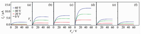
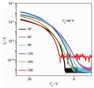
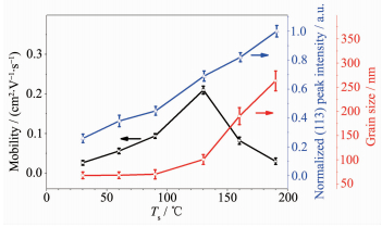
Fig. 4 shows the transfer characteristics of C60 TFTs prepared under different Ts. From the transfer curves, the carrier mobility are extracted for each device, and the relationship between the mobilities and Ts are shown in Fig. 6. In order to make clear of the correlation of the mobilities with the corresponding crystallinity and morphologies of the C60 films, the changes of (113) peak intensity and grain sizes with Ts are re-plotted here. It is seen that, for C60 films with Ts below 130 ℃, the mobilities increase from 0.026 to 0.211 cm2·V-1·s-1 with increasing Ts. With further increasing Ts to 160 and 190 ℃, mobilities decrease to 0.082 and 0.030 cm2·V-1·s-1, respectively. Because of the unchanged grain sizes of C60 films deposited under 30, 60 and 90 ℃, the increase of mobilities could be attributed to the increased crystallinities of films. When Ts is up to 130 ℃, the larger mobility was achieved mainly due to the higher crystallinities despite the slightly increased grain sizes. Interestingly, for the films with Ts of 160 and 190 ℃, despite the increases in the crystallinities, remarkable decreased mobilities are obtained, which should be related the obviously increased grain sizes. These results suggest the different grain-boundary effect for the spherical C60 molecules from that for the planar molecules, such as CuPc, pentacene, TIPS-pentacene, perylene bisimide and oligothiophene[14-25]. For the planar molecules, the grain boundary is a crucial barrier for the carrier transport, since the intermolecular charge hopping across the grain boundaries is less efficient than that within the grains. Thus, reducing the grain boundaries by increasing grain sizes is a promising approach to improve charge transport and mobility. However, for the C60 samples with Ts of 160 and 190 ℃, the larger grain sizes of spherical C60 films lead to the lower mobilitis, which is interesting and worth further investigating.
In order to reveal the influence of grain sizes on the mobilities of C60 films, the samples with similar crystallinities and different grain sizes are needed. In our previous study, we have demonstrated that higher deposition pressure in vacuum deposition could lead to the larger grain sizes of C60 films with unchanged crystallinities and molecular packing[16]. Thus, the C60 films with deposition pressure of 1×10⁻¹ Pa and Ts of 130 ℃ are deposited and investigated. In contrast to the C60 films with deposition pressure of 1×10⁻⁴ Pa (Fig. 2Ad and 2Bd), the samples of 1×10⁻¹ Pa show the unchanged crystallinities and increased grain sizes, as shown in Fig. 6. The C60 films with deposition pressure of 1×10⁻¹ Pa have a mobility of 0.030 cm2·V-1·s-1, which is lower than the value of samples with deposition pressure of 1×10⁻⁴ Pa. Due to the unchanged crys-tallinities, the decrease of mobility should be corrected to the increased grain size.
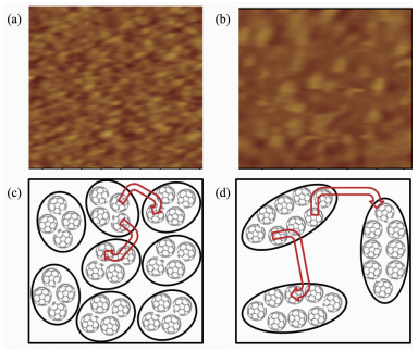
As known, the performance of OTFTs is determined by the crystalline order and grain sizes of the first few molecular layers of the semiconductor near the semiconductor/dielectric interface. To ascertain the grain sizes of the C60 layers at C60/SiO2 interface, two C60 films of 10 nm thickness were deposited on SiO2 at deposition pressure of 1×10⁻⁴ and 1×10⁻¹ Pa, respectively. From the corresponding AFM images in Fig. 7a and b, it is seen that, the 10 nm C60 films deposited under 1×10⁻⁴ Pa have a lot of small grains, while some larger grains are observed for the films of 1×10⁻¹ Pa. This confirmed that larger grain sizes of C60 films result in the lower mobilities. The possible mechanism for the effect of grain size on mobility of C60 films is proposed in Fig. 7c and d. For the spherical C60 molecules, carrier could be effectively transported through nearest-neighbor hopping between molecules[26]. So the films with small and close grains are advantageous to effective charge transport (Fig. 7c). For the films with large grain size, it is difficult to realize the nearest-neighbor hopping between grains molecules, due to the large spacing between the grains (Fig. 7d). Thus, the grain boundary is not a serious barrier for the charge transport, and the larger grain size could lead to the lower mobility in C60 TFTs.
In summary, C60 films have been prepared on SiO2 substrates by vacuum deposition under different substrate temperature ranging from ranging from 30 to 190 ℃ and deposition pressure of 1×10⁻⁴ and 1×10⁻¹ Pa. The experimental results indicate that the crystallinity and grain size of the C60 films thereof the mobility of the obtained TFTs could be effectively regulated by tuning substrate temperature and deposi-tion pressure. A clear correlation of mobility with crystallinity and grain size of the C60 film is established. It is found that, both the crystallinity and the grain size of the C60 films increase with increasing substrate temperature. And the grain sizes of the films increase and the crystallinity keep almost unchanged with increasing deposition pressure. The mobilities of the C60 films are closely correlated with the crystall-inity and grain size. The increased crystallinity of the C60 films gives the improved mobility. Different from the films of planar organic semiconducrors molecules, for the spherical C60 molecules films, the larger grain size could lead to the lower mobility. This study is helpful for the understanding of the charge transfer process and improving the performance of OTFTs.
Someya T, Bao Z, Malliaras G G. Nature, 2016, 540:379-385 doi: 10.1038/nature21004
Nomura K, Ohta H, Takagi A, et al. Nature, 2004, 432:488-492 doi: 10.1038/nature03090
Baeg K, Khim D, Kim J, et al. Adv. Funct. Mater., 2012, 22: 2915-2926 doi: 10.1002/adfm.v22.14
Someya T, Sekitani T, Iba S, et al. Proc. Natl. Acad. Sci. USA, 2004, 101:9966-9970 doi: 10.1073/pnas.0401918101
Rotzoll R, Mohapatra S, Olariu V, et al. Appl. Phys. Lett., 2006, 88:123502 doi: 10.1063/1.2186384
Li Y, Liu Q, Wang X Z, et al. Sci. China. Tech. Sci., 2012, 55:417-420 doi: 10.1007/s11431-011-4693-5
Sun X, Zhang L, Di C, et al. Adv. Mater., 2011, 23:3128-3133 doi: 10.1002/adma.v23.28
Virkar A, Mannsfeld S, Toney M F, et al. Adv. Funct. Mater., 2009, 19:1962-1970 doi: 10.1002/adfm.v19:12
李谊, 刘琪, 蔡婧, 等.无机化学学报, 2014, 11:2621-2625 http://www.wjhxxb.cn/wjhxxbcn/ch/reader/view_abstract.aspx?flag=1&file_no=20141124&journal_id=wjhxxbcnLI Yi, LIU Qi, CAI Jing, et al. Chinese J. Inorg. Chem., 2014, 11:2621-2625 http://www.wjhxxb.cn/wjhxxbcn/ch/reader/view_abstract.aspx?flag=1&file_no=20141124&journal_id=wjhxxbcn
Kelley T W, Boardman L D, Dunbar T D, et al. J. Phys. Chem. B, 2003, 107:5877-5881 doi: 10.1021/jp034352e
Facchetti A, Letizia J, Yoon M H, et al. Chem. Mater., 2004, 16:4715-4727 doi: 10.1021/cm0495008
Zhang X R, Richter L J, DeLongchamp D M, et al. J. Am. Chem. Soc., 2011, 133:15073-15084 doi: 10.1021/ja204515s
Li L, Hu W, Fuchs H, et al. Adv. Energy Mater., 2011, 1: 188-193 doi: 10.1002/aenm.201000021
Bao Z, Lovinger A J, Dodabalapur A. Adv. Mater., 1997, 9: 42-44 doi: 10.1002/(ISSN)1521-4095
Horowitz G, Hajlaoui M E. Adv. Mater., 2000, 12:1046-1050 doi: 10.1002/(ISSN)1521-4095
Li Y, Chen S, Liu Q, et al. J. Phys. Chem. C, 2012, 116:4287-4292 doi: 10.1021/jp210547j
Yang S Y, Shin K, Park C E. Adv. Funct. Mater., 2005, 15: 1806-1814 doi: 10.1002/(ISSN)1616-3028
Bräuer B, Kukreja R, Virkar A, et al. Org. Electron., 2011, 12:1936-1942 doi: 10.1016/j.orgel.2011.08.007
Ye R, Baba M, Ohishi Y, et al. Mol. Cryst. Liq. Cryst., 2006, 444:203-210 doi: 10.1080/15421400500364972
Li Y, Chen S, Liu Q, et al. J. Phys. Chem. C, 2014, 118: 14218-14226 doi: 10.1021/jp5035954
Hu Y, Qi Q, Jiang C. Appl. Phys. Lett., 2010, 96:133311 doi: 10.1063/1.3374887
Schmidt R, Oh J H, Sun Y S, et al. J. Am. Chem. Soc., 2009, 131:6215-6228 doi: 10.1021/ja901077a
Acton O, Ting G G, Shamberger P J, et al. ACS Appl. Mater. Interfaces, 2010, 2:511-520 doi: 10.1021/am9007648
Yakuphanoglu F, Gunduz B. Synth. Met., 2012, 162:1210-1239 doi: 10.1016/j.synthmet.2012.04.034
Chen J, Tee C K, Shtein M, et al. J. Appl. Phys., 2008, 103: 114513 doi: 10.1063/1.2936978
Sung C, Kekuda D, Chu L F, et al. Adv. Mater., 2009, 21: 4845-4849 doi: 10.1002/adma.200901215
Kobayashi S, Takenobu T, Mori S, et al. Sci. Technol. Adv. Mater., 2003, 4:371-375 doi: 10.1016/S1468-6996(03)00064-0
Anthopoulos T D, Singh B, Marjanovic N, et al. Appl. Phys. Lett., 2006, 89:213504 doi: 10.1063/1.2387892

Figure 2 Characteristic XRD patterns (A) and AFM images (B) of the 40 nm C60 films deposited under different Ts of 30, 60, 90, 130, 160 and 190 ℃ (a~f), respectively

Figure 3 Output (Id-Vd) characteristics of C60 TFTs prepared under different Ts of 30, 60, 90, 130, 160 and 190 ℃ (a~f)

Figure 4 Transfer (Id-Vg) characteristics of C60 TFTs prepared under different Ts of 30, 60, 90, 130, 160 and 190 ℃

Figure 5 Carrier mobilities, grain sizes, and crystallinity ((113) peak intensity) of C60 thin films as functions of Ts

Figure 6 Characteristic XRD pattern (a) and AFM image (b) of the 40 nm C60 films deposited under 1×10⁻¹ Pa and 130 ℃

 扫一扫看文章

扫一扫关注我们
 下载:
下载:

 下载:
下载:

 下载:
下载: